Electrostatic discharge protection structure based on SOI process

An electrostatic discharge protection and ESD protection technology, which is applied in the direction of circuits, electrical components, and electric solid devices, can solve problems such as poor ESD protection performance, improve electrostatic discharge protection capabilities, prevent overheating and burnout, and eliminate device breakdown and burnout The effect of the phenomenon

Active Publication Date: 2020-07-10
SHANGHAI INST OF MICROSYSTEM & INFORMATION TECH CHINESE ACAD OF SCI
View PDF7 Cites 2 Cited by
  • Summary
  • Abstract
  • Description
  • Claims
  • Application Information

AI Technical Summary

Problems solved by technology

[0005] The object of the present invention is to provide a kind of electrostatic discharge protection structure based on SOI process, in order to overcome the technical problem of the poor ESD protection performance of the electrostatic discharge protection structure based on SOI process in the prior art

Method used


Image

  • Electrostatic discharge protection structure based on SOI process
  • Electrostatic discharge protection structure based on SOI process

Examples


Embodiment 1

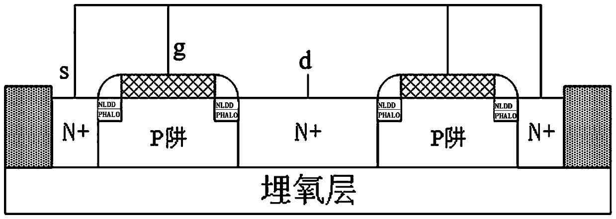
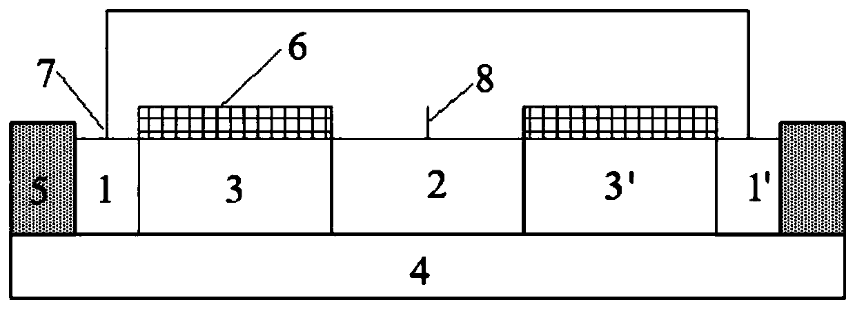
[0026] In this example, see figure 2 , provides an electrostatic discharge protection structure based on SOI technology. It should be noted that the drawings are not drawn to scale, and the drawings are all in a very simplified form, which is only used to facilitate and clearly illustrate the purpose of this embodiment . The electrostatic discharge protection structure based on the SOI process of this embodiment includes an SOI substrate and an ESD protection device located on the SOI substrate; the ESD protection device includes a first conductive region 1, a second conductive region 2 and a third conductive region 3, the first A conductive region 1, a second conductive region 2 and a third conductive region 3 are located on the same plane, and the third conductive region 3 is respectively in contact with the first conductive region 1 and the second conductive region 2; the first conductive region 1 is formed with a An electrode 7, a second electrode 8 is formed on the seco...

Embodiment 2

[0037] In this embodiment, continue to refer to figure 2 , providing an electrostatic discharge protection structure based on SOI technology. The difference between the electrostatic discharge protection structure based on the SOI process of this embodiment and the first embodiment is that the first conductivity type is P-type, the second conductivity type is N-type, and the ESD protection device is a PMOS transistor.

[0038] In a preferred embodiment, a drain region (P+)-N well-source region (P+) parasitic transistor can be formed inside the ESD protection device. When an ESD pulse is applied to the PAD, the parasitic transistor PNP is turned on, and the leakage Discharge ESD current, so as to protect other protected circuits from electrostatic discharge.

[0039] In a specific implementation manner, the N-type well region, the P+-type source region and the P+-type drain region are all formed deep into the buried oxide layer 4 .

[0040] In this embodiment, as an example,...

Embodiment 3

[0043] In this embodiment, continue to refer to figure 2 , providing an electrostatic discharge protection structure based on SOI technology. The difference between the electrostatic discharge protection structure based on the SOI process of this embodiment and Embodiment 1 is that the first conductive region 1 is formed as the first conductive type ion implantation region, and the second conductive region 2 is formed as the second conductive type ion implantation region. The third conductive region 3 is formed as a well region of the first conductive type or the second conductive type, and the ESD protection device is configured as a diode.

[0044] In a specific implementation manner, the first conductivity type is P-type, and the second conductivity type is N-type, forming a PNP diode. When an ESD pulse is applied to the anode, the diode is turned on to discharge the ESD current. The first electrode 7 is a positive electrode, and the second electrode 8 is a negative elec...


PUM


Abstract

The invention discloses an electrostatic discharge protection structure based on an SOI process. The electrostatic discharge protection structure comprises an SOI substrate and an ESD protection device located on the SOI substrate. The ESD protection device comprises a first conductive area, a second conductive area and a third conductive area, wherein the first conductive area, the second conductive area and the third conductive area are located on the same plane, and the third conductive area makes contact with the first conductive area and the second conductive area respectively. A first electrode is formed on the first conductive area, a second electrode is formed on the second conductive area, a silicide barrier layer is arranged above the third conductive area, and the first electrode and the second electrode are isolated by the silicide barrier layer. According to the invention, the first electrode and the second electrode are isolated through the silicide barrier layer, and when ESD impact occurs, the parasitic triode is conducted to discharge ESD current, so a protected circuit is protected. According to the electrostatic discharge protection structure, an ESD current canbe enabled to flowto a deeper region, and the electrostatic discharge protection capability of the device can be effectively improved.

Description

technical field [0001] The invention relates to the technical field of integrated circuits, in particular to an electrostatic discharge protection structure based on SOI technology. Background technique [0002] Static electricity is an objective natural phenomenon, which can be produced in many ways, such as contact, friction, induction between electrical appliances, etc. Static electricity is characterized by long-term accumulation, high voltage, low power, small current and short action time. Static electricity poses serious hazards in at least two areas. Friction electrification and human body static electricity are two major hazards in the electronics industry, which often cause unstable operation or even damage of electronic and electrical products. Electrostatic discharge (ESD: Electrostatic Discharge) protection is an important link in integrated circuit (IC) design. As the technology becomes more and more advanced, especially in the new SOI (Silicon-On-Insulator, ...

Claims


Application Information

Patent Timeline
Patent Type & Authority Applications(China)
IPC IPC(8): H01L27/02
CPCH01L27/0251H01L27/0259
Inventor 单毅董业民陈晓杰
Owner SHANGHAI INST OF MICROSYSTEM & INFORMATION TECH CHINESE ACAD OF SCI
Why Eureka
Try Eureka