Circuit board and method of manufacturing the same

a technology of circuit boards and components, applied in the direction of coupling contact members, coupling device connections, coupling protective earth/shielding arrangements, etc., can solve the problems of increasing the complexity of the manufacturing process, the inability to place other components in time, and the inability to manufacture the sam

Inactive Publication Date: 2008-04-03
HONDA MOTOR CO LTD
View PDF6 Cites 57 Cited by
  • Summary
  • Abstract
  • Description
  • Claims
  • Application Information

AI Technical Summary

Benefits of technology

[0017] In another aspect of the present invention, in the method of manufacturing the circuit board including the above-mentioned steps, the cylindrical recess is formed before the conductive terminal is fitted into the through hole, and the conductive terminal is electrically connected to the partially exposed surface of the conductive layer, which is exposed by forming the cylindrical recess. The circuit board is heated to a predetermined te

Problems solved by technology

However, a more complicated manufacturing process is required to provide the large number of the through hole parts 65.
A

Method used


Image

  • Circuit board and method of manufacturing the same
  • Circuit board and method of manufacturing the same
  • Circuit board and method of manufacturing the same

Examples


first embodiment

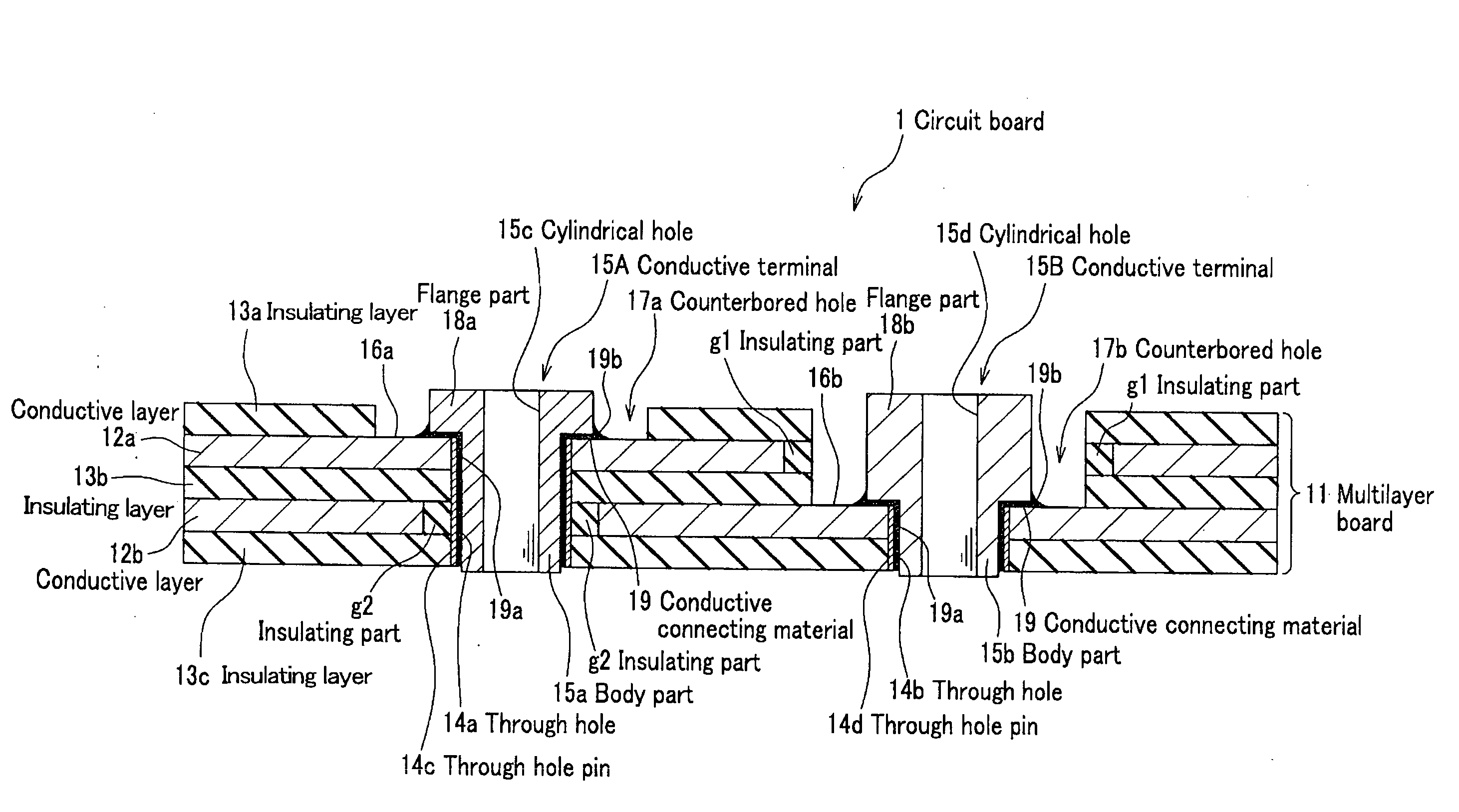
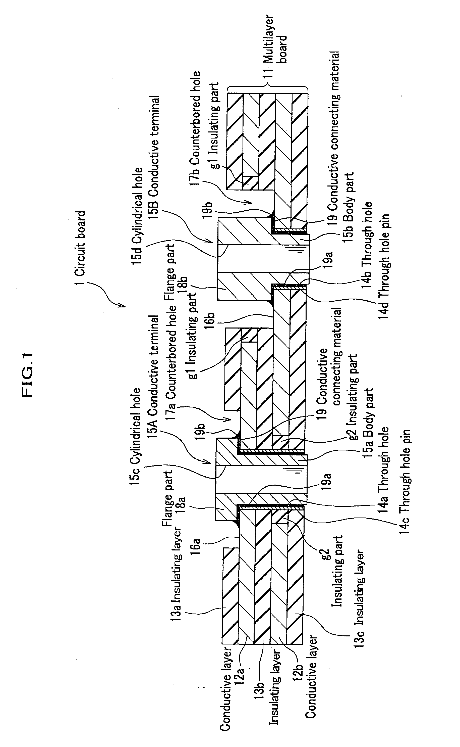
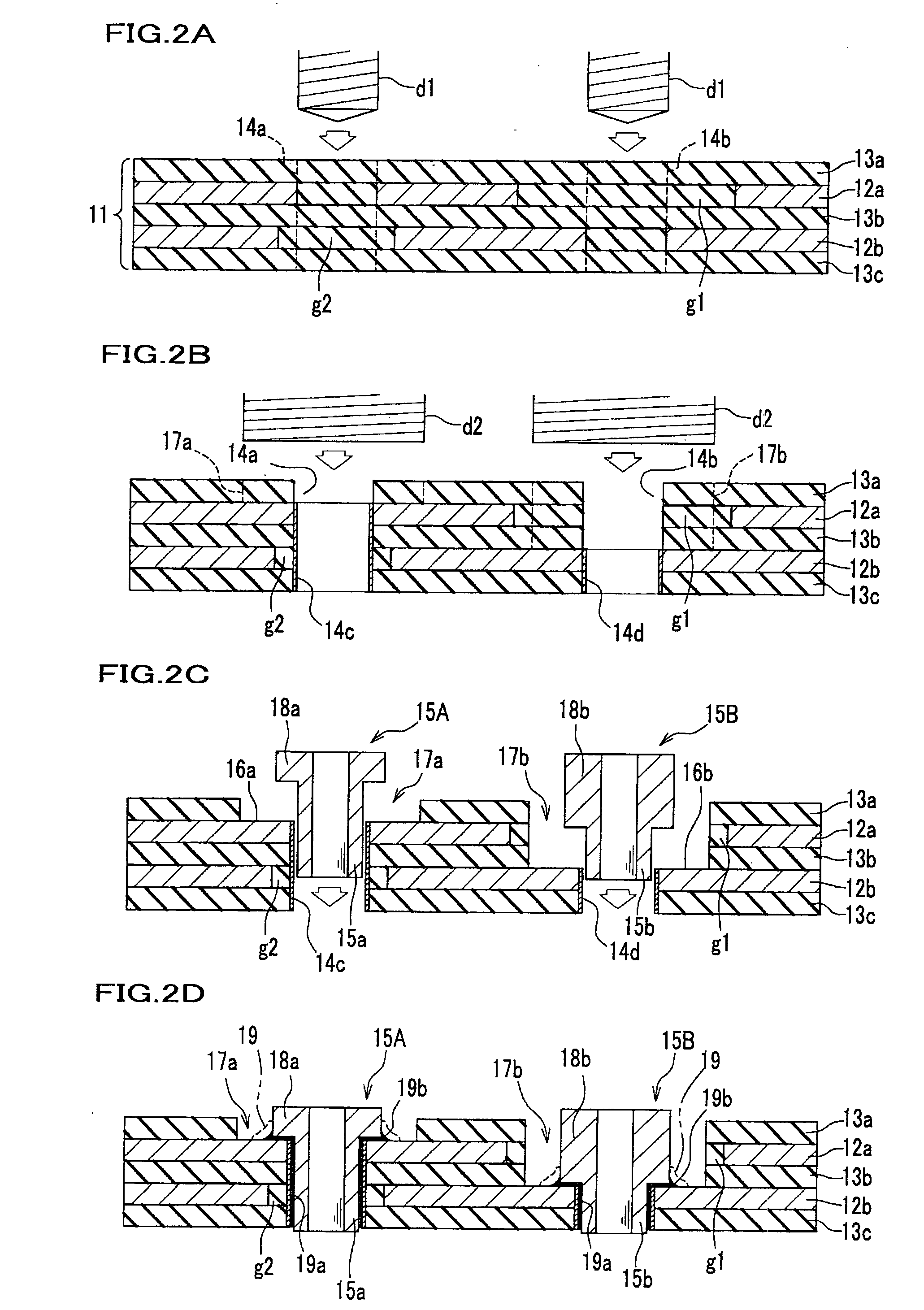
[0030] As shown in FIG. 1, the circuit board 1 includes a multilayer board 11, conductive terminals 15A,15B, and through hole pins 14c,14d.

[0031] The multilayer board 11 is formed by alternately stacking insulating layers 13a,13b,13c and conductive layers 12a,12b. The insulating layers 13a,13b,13c are thin layers made of insulating material such as glass epoxy resin. The conductive layers 12a,12b are thin layers made of copper, for example, and have predetermined circuit patterns therein.

[0032] The insulating layers 13a,13b,13c and the conductive layers 12a,12b have each suitable thickness according to material thereof, a magnitude of a current which is to flow through the conductive layers 12a,12b, and a size of the circuit board 1.

[0033] The multilayer board 11 has cylindrical through holes 14a,14b, which penetrate the multilayer board 11 at predetermined positions thereof; and counterbored holes (cylindrical recesses) 17a,17b to be described later, which penetrate the insulati...

second embodiment

[0062] Next is described a second embodiment with reference to FIG. 5A to FIG. 5D. FIG. 5A to FIG. 5D are sequential cross sectional views showing a first step to a fifth step as key steps in the method of manufacturing a circuit board. A configuration of the second embodiment is the same as that of the first embodiment shown in FIG. 1, except that the number of layers stacked in the circuit board is different, and that a pair of counterbored holes are formed on both an upper surface and a lower surface of the circuit board. Descriptions of a configuration and a process which have been already mentioned in the first embodiment will be omitted herefrom.

[0063] As shown in FIG. 5C and FIG. 5D, a circuit board 2 according to the second embodiment includes: a multilayer board 21, through hole pins 24c,24d, and conductive terminals 32A,32B, latter two of which are placed in the multilayer board 21.

[0064] The multilayer board 21 is configured such that insulating layers 23a,23b,23c,23d,2...

third embodiment

[0080] Next are described a circuit board and key steps of a method of manufacturing the circuit board according to a third embodiment with reference to FIG. 6A, FIG. 6B and FIG. 6C. FIG. 6A, FIG. 6B and FIG. 6C are sequential cross sectional views each showing a key step of the method of manufacturing the circuit board according to the third embodiment.

[0081] A configuration of the third embodiment is the same as that of the embodiments described above, except that no through hole pin is used, and that second flange parts are provided in the third embodiment. Difference between the third and the other embodiments is mainly described herein, and description of same configurations is omitted herefrom.

[0082] As shown in FIG. 6A, FIG. 6B and FIG. 6C, a circuit board 3 includes a multilayer board 41; first counterbored holes 47a,47b and second counterbored holes 49a,49b each formed concentric with through holes 44a,44b, respectively, the through holes 44a,44b penetrating the multilaye...


PUM

PropertyMeasurementUnit
Electrical conductoraaaaaaaaaa
Weightaaaaaaaaaa

Abstract

A circuit board and a method of manufacturing the same are provided. The circuit board includes: a multilayer board in which a plurality of conductive layers with desired patterns formed therein, and a plurality of insulating layers are stacked; a plurality of through holes penetrating the multilayer board; cylindrical recesses each formed around a through hole corresponding thereto, having a diameter larger than that of the through hole, having a depth from an outermost surface of the insulating layer to a surface of the conductive layer for electrical connection, and partially exposing the surface of the predetermined conductive layer; and a plurality of conductive terminals fitted into the through holes.

Description

CROSS REFERENCE TO RELATED APPLICATIONS [0001] This application claims the benefit of Japanese Patent Application No. 2006-235609 filed on Aug. 31,2006, the disclosure of which is incorporated herein by reference. BACKGROUND OF THE INVENTION [0002] 1. Field of the Invention [0003] The present invention relates to a circuit board and a method of manufacturing the same, and more specifically, to a circuit board, which allows a large electric current to flow through a circuit pattern therein, and a method of manufacturing the same. [0004] 2. Description of the Related Art [0005] In general, use of electronic circuits has been rapidly expanded to such fields as industry machines and automobile parts. In particular, a composite circuit board has been widely used in an inverter circuit, a control circuit of a servo motor, a power supply unit, or the like. In the composite circuit board, a thin circuit pattern for a small current (for a signal) and a thick circuit pattern for a large curre...

Claims


Application Information

Patent Timeline
IPC IPC(8): H05K3/46H05K1/11H05K3/36
CPCH05K3/0047H05K3/325H05K3/3447H05K3/4046Y10T29/49165H05K2201/10401H05K2201/10409H05K2201/10962Y10T29/49126H05K2201/09845
Inventor WATANABE, YASUTOFUJITA, HIROYUKIWATANABE, KUNIO
Owner HONDA MOTOR CO LTD
Why Eureka
Try Eureka