Semiconductor electrostatic discharge protection device

An electrostatic discharge protection, semiconductor technology, applied to semiconductor devices, semiconductor/solid-state device components, circuits, etc., can solve problems such as crashes and permanent failure of transistor units

Inactive Publication Date: 2015-06-03
UNITED MICROELECTRONICS CORP
View PDF0 Cites 3 Cited by
  • Summary
  • Abstract
  • Description
  • Claims
  • Application Information

AI Technical Summary

Problems solved by technology

[0004] However, the traditional grounded gate n-type metal-oxide-semiconductor transistor unit is prone to secondary snapback collapse due to the base push-out effect of the parasitic NPN bicarrier junction transistor. To make the excessive leakage current pass through the emitter and ground base of the parasitic double carrier junction transistor, and then conduct to the ground f...

Method used


Image

  • Semiconductor electrostatic discharge protection device
  • Semiconductor electrostatic discharge protection device
  • Semiconductor electrostatic discharge protection device

Examples


Embodiment Construction

[0058] The invention provides a semiconductor electrostatic discharge protection device, which can reduce the leakage current from being conducted to the ground through the element substrate, and improve the electrostatic discharge protection capability of the semiconductor electrostatic discharge protection device. In order to make the above and other objects, features and advantages of the present invention more comprehensible, several preferred embodiments will be described in detail below together with the accompanying drawings.

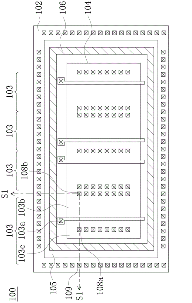
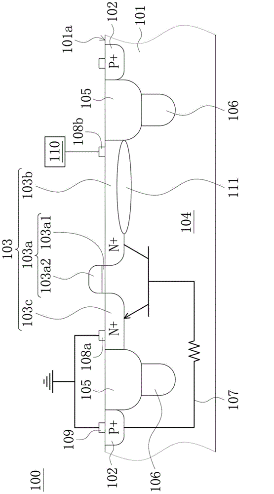
[0059] Please refer to Figure 1A with 1B , Figure 1A It is a schematic top view of the structure of the semiconductor electrostatic discharge protection device 100 according to an embodiment of the present invention. Figure 1B is extended Figure 1A A cross-sectional schematic diagram of a partial structure of the semiconductor ESD protection device 100 shown by the tangent line S1 of . Among them, the semiconductor electrostatic discharge pr...


PUM


Abstract

The invention discloses a semiconductor electrostatic discharge protection device, which comprises a first electric transistor, a second electric trap region, a second electric protection ring and a semiconductor separation region, wherein the first electric transistor is formed in the second electric trap region, the second electric protection ring surrounds the first electric transistor, the semiconductor separation region is positioned between the first electric transistor and the second electric protection ring, and surrounds the first electric transistor, and in addition, the semiconductor separation region is a non-doping region, a first electric doping region or a second electric doping region with the doping concentration being smaller than that of the second electric trap region.

Description

technical field [0001] The invention relates to a semiconductor integrated circuit element, and in particular to a semiconductor electrostatic discharge protection device. Background technique [0002] Electrostatic discharge is the migration of electrostatic charges on non-conductive surfaces through conductive materials. Since electrostatic voltage is usually quite high, electrostatic discharge can easily damage the substrate and other components of an integrated circuit. In order to protect the integrated circuit from being damaged by ESD, a device with the function of conducting the ESD current to the ground is integrated into the integrated circuit. [0003] Take the grounded gate n-type metal-oxide-semiconductor conductor Gate Grounded n-type Metal-Oxide-Semiconductor (GGNMOS) transistor unit as an example, its gate, source and element substrate are grounded, when electrostatic discharge occurs (ESD zapping) , the snapback causes the grounded gate n-type metal-oxide-...

Claims


Application Information

Patent Timeline
IPC IPC(8): H01L23/60
Inventor 陈俞均王畅资唐天浩
Owner UNITED MICROELECTRONICS CORP
Why Eureka
Try Eureka