Integrated circuit with electrostatic discharge protecting circuit

An electrostatic discharge protection, integrated circuit technology, applied in emergency protection circuit devices, emergency protection circuit devices for limiting overcurrent/overvoltage, circuits, etc. and other problems, to achieve the effect of improving electrostatic discharge protection capability, reducing conduction inconsistency, and reducing layout area.

Active Publication Date: 2009-09-02
RAYDIUM SEMICON
View PDF0 Cites 2 Cited by
  • Summary
  • Abstract
  • Description
  • Claims
  • Application Information

AI Technical Summary

Problems solved by technology

[0008] However, due to the turn-on uniformity characteristics of the NMOS transistor 132 and the PMOS transistor 134, if the NMOS transistor in the power clamping circuit 130 When the size of 132 or PMOS transistor 134 increases, its electrostatic protection ability cannot be enhanced consistently, so a new electrostatic discharge protection mechanism is urgently needed to achieve the enhancement of its electrostatic discharge when the circuit size increases. Discharge protection capability

Method used


Image

  • Integrated circuit with electrostatic discharge protecting circuit
  • Integrated circuit with electrostatic discharge protecting circuit
  • Integrated circuit with electrostatic discharge protecting circuit

Examples


Embodiment Construction

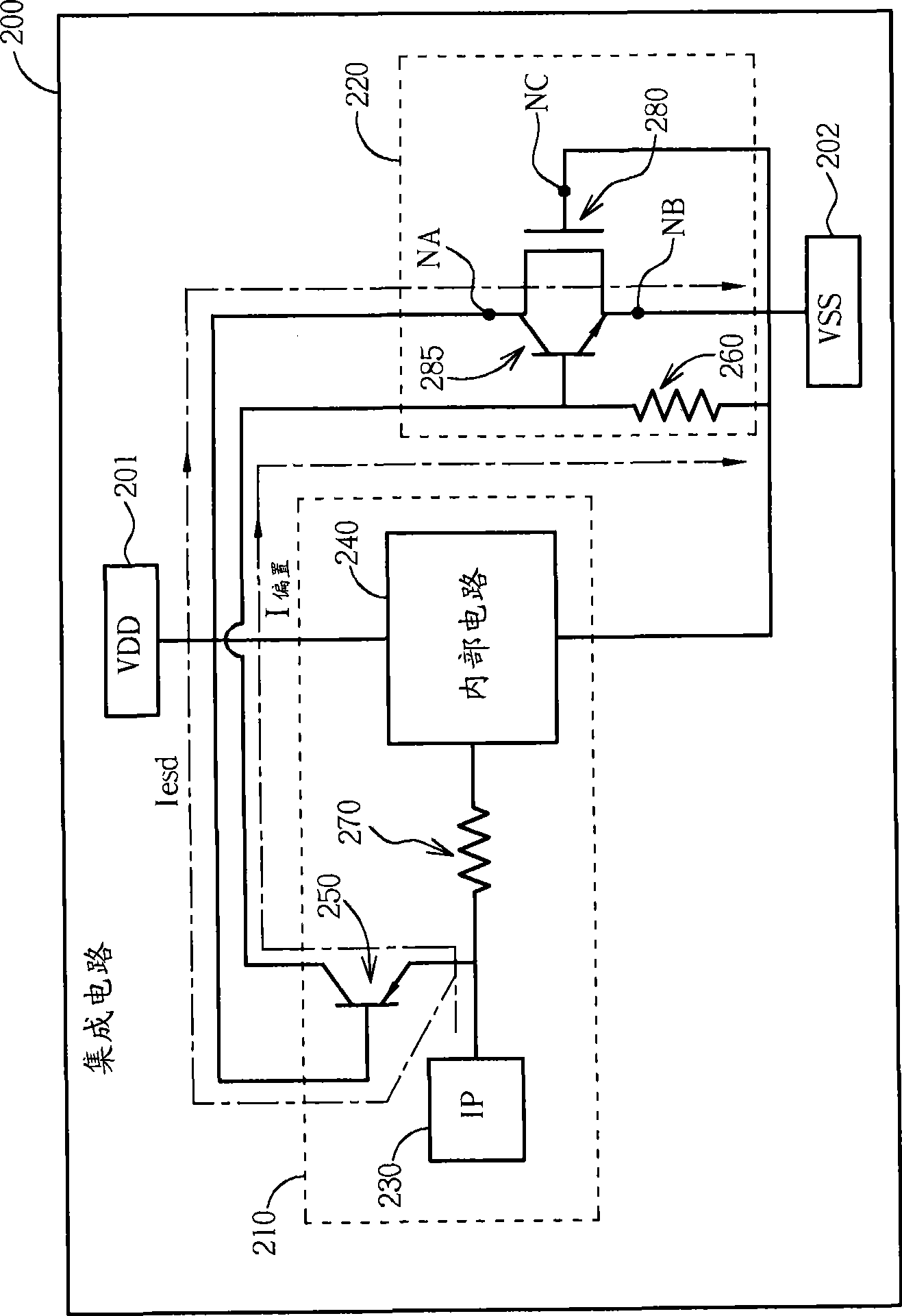
[0022] see figure 2 , figure 2 It is a schematic diagram of an integrated circuit 200 with an ESD protection circuit according to the first embodiment of the present invention. The integrated circuit 200 includes (but not limited to) a first power pad 201, a second power pad 202, at least one circuit module 210, and a power clamping circuit 220. In addition, in the integrated circuit 200, the power clamping circuit 220 also has a first Parasitic bipolar junction transistor 285 . In addition, please note that in this embodiment, the first power pad 201 is a VDD terminal, and the second power pad 202 is a VSS terminal.

[0023] Such as figure 2 As shown, the circuit module 210 includes a signal pad 230 , an internal circuit 240 and a first BJT 250 . In addition, if the design requires, the circuit module 210 may also include an impedance element 270 (such as figure 2shown). For the convenience of description, in the following description, the signal pad 230 is an input...


PUM


Abstract

The invention discloses an integrated circuit with an electrostatic discharge protecting circuit. The integrated circuit comprises a first power source connecting pad, a second power source connecting pad, at least one circuit module and a power source clamping circuit. The circuit module comprises a signal connecting pad, an internal circuit and a first bipolar junction transistor. A first parasitic resistance is arranged between the collector of the first bipolar junction transistor and the second power source connecting pad. The power source clamping circuit comprises at least one first metal-oxide-semiconductor transistor and at least one first parasitic bipolar junction transistor.

Description

technical field [0001] The present invention relates to an integrated circuit, in particular to an integrated circuit with an electrostatic discharge protection circuit, and the integrated circuit applies bipolar junction transistor and substrate trigger (substrate trigger) technology to enhance / improve the electrostatic protection capability. Background technique [0002] With the advancement of science and technology, the technology of integrated circuit technology has also been continuously developed. As known to those skilled in the field of integrated circuits, various electronic circuits can be integrated / formed on a chip, and in order to enable the chip to receive an external voltage source (such as a bias power supply) and exchange For data, conductive pads are provided on the chip. For example, in order to transmit the bias voltage, a power pad (power pad), that is, a VDD terminal and a VSS terminal, may be provided on the chip. In addition, signal pads, namely in...

Claims


Application Information

Patent Timeline
Patent Type & Authority Applications(China)
IPC IPC(8): H02H9/00H01L23/60
Inventor 杨景荣吴坤泰
Owner RAYDIUM SEMICON
Why Eureka
Try Eureka