Protective cover plate and electronic device applying same
A technology for protecting cover plates and electronic devices, which can be used in electrical equipment casings/cabinets/drawers, telephone communications, electrical components, etc., and can solve problems such as accelerated penetration and unreasonableness.
- Summary
- Abstract
- Description
- Claims
- Application Information
AI Technical Summary
Problems solved by technology
Method used
Image
Examples
no. 1 example
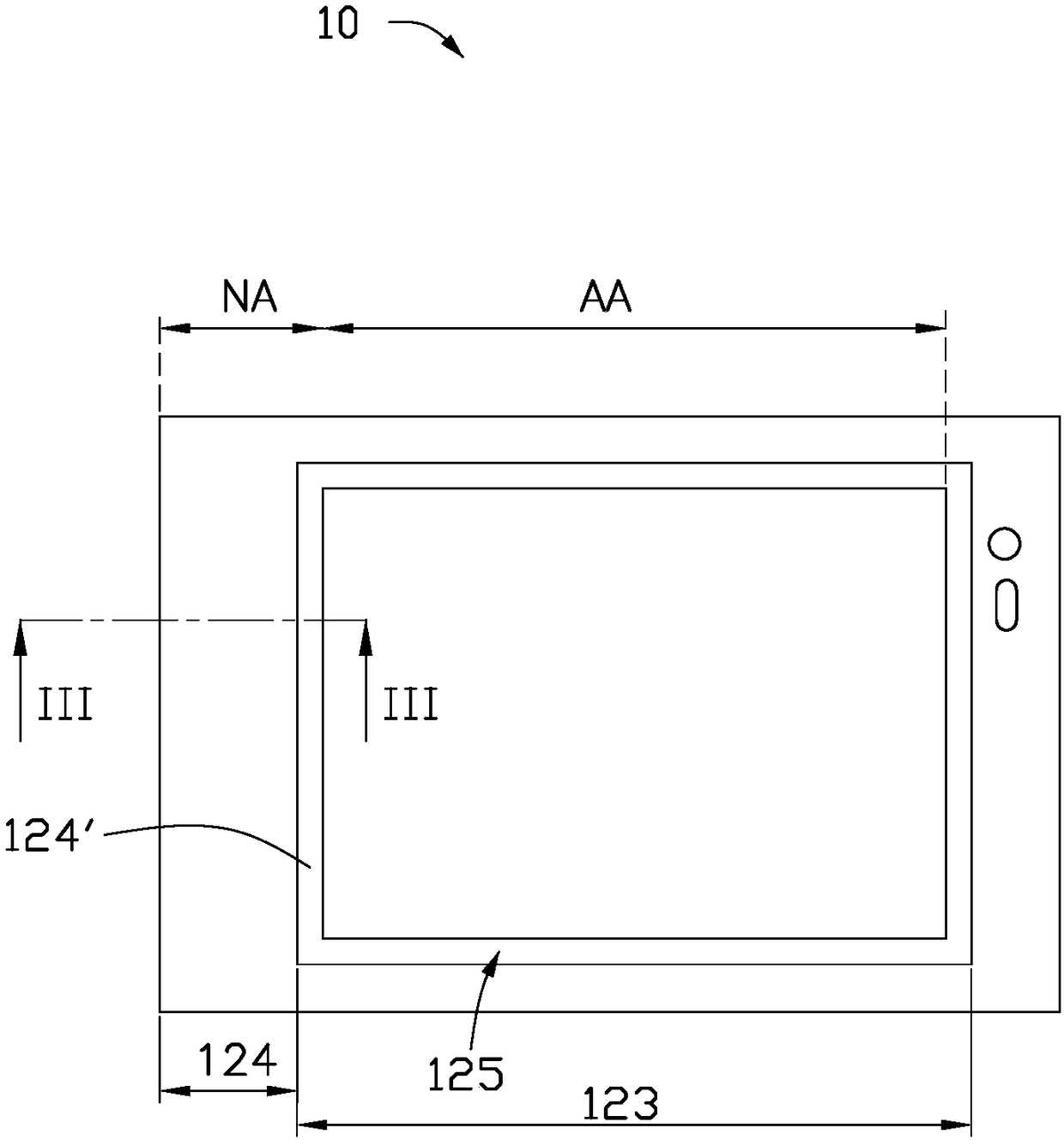
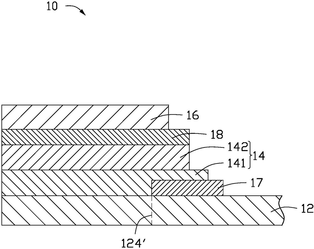
[0024] Please refer to figure 2 and image 3 , figure 2 Shown is a schematic plan view of the protective cover of the first embodiment of the present invention. image 3 shown as figure 2 The schematic cross-sectional view of the protective cover along the section line III-III, and in order to make the illustration more clearly presented, image 3 Only a part of the protective cover is shown enlarged.
[0025] In the present invention, the protective cover 10 can be applied to cover the surface of the electronic device 1 with touch display function, so as to protect the display and touch elements of the electronic device 1 . In one embodiment, the touch element of the electronic device is an add-on touch panel, and the touch surface of the touch panel used to be in contact with a touch object such as a finger is bonded to the protective cover 10 , and is connected to the touch panel. The other surface opposite to the control surface is attached to the display panel. I...
no. 2 example
[0037] see Figure 4 , Figure 4 It is a schematic cross-sectional view of the second embodiment of the present invention. The protective cover of the second embodiment has the same schematic plan view as the protective cover of the first embodiment. Therefore, image 3 and Figure 4 are all along figure 2 Schematic diagram of the cross section in section line II-II.
[0038] When describing the protective cover plate 10 of this embodiment, the same elements use the same reference numerals as in the previous embodiment. Such as Figure 4 As shown, the protective cover 10 further includes a secondary sacrificial layer 19 disposed on the surface of the secondary shielding layer 17 away from the substrate 12 . The secondary sacrificial layer 19 is disposed between the secondary shielding layer 17 and the first decoration layer 141 , and opposite surfaces of the secondary sacrificial layer 19 are in contact with the secondary shielding layer 17 and the first decoration layer...
PUM
 Abstract
Description
Claims
Application Information


