FPGA-based TDC realization method
An implementation method and technology of delay chain, which can be used in image data processing, program control, instruments, etc., and can solve problems such as DNL influence and regional delay change.
- Summary
- Abstract
- Description
- Claims
- Application Information
AI Technical Summary
Benefits of technology
Problems solved by technology
Method used
Image
Examples
specific Embodiment
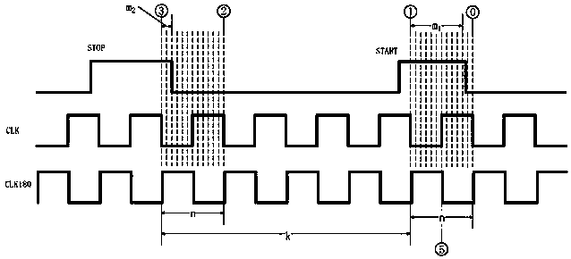
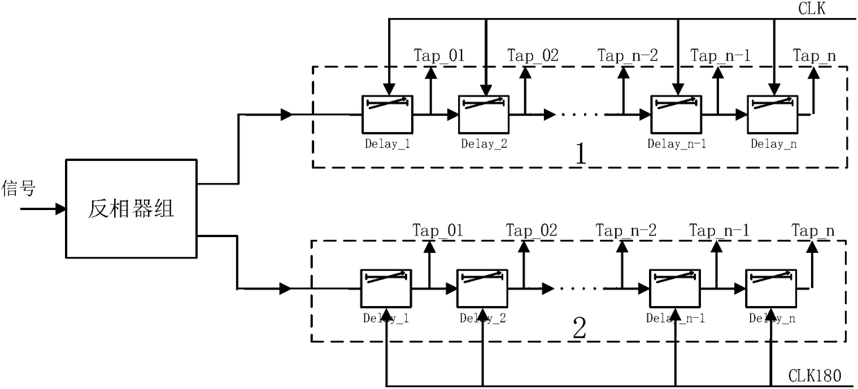
[0019] Use the clock management tool (DCM) of FPGA to generate two 400MHz clocks with a difference of 180°, CLK and CLK180, which are distributed in two clock regions. On these two clock regions, deploy the same delay chain program. An inverter group is added to the signal input end, and the delay time of the input signal reaching the two modules is adjusted so that the difference does not exceed 1 ns. By adopting the method of the present invention, the number of delay chains in each clock domain can be doubled, that is, each delay chain requires 20 delay units. There are 49-50 delay units in each BANK column of the FPGA, and there is sufficient layout and wiring space to realize the above design.
[0020] The delay chain uses the CARRY4 carry unit of the FPGA, and the CIN of each carry unit is connected to the COUT of the next unit to form a delay chain. The COUT of each delay unit is output to the flip-flop as a tap, and the clock of the local clock domain is used for dat...
PUM
 Abstract
Description
Claims
Application Information

