Active recognition type liquid crystal display device and manufacturing method thereof

A liquid crystal display device, active identification technology, applied in instruments, computing, electrical digital data processing and other directions, can solve the problems of increasing the thickness of the display, difficult to distinguish, reducing the display effect, etc., to achieve the effect of active identification

Active Publication Date: 2020-12-25
HUIZHOU CHINA STAR OPTOELECTRONICS TECHNOLOGY CO LTD
View PDF7 Cites 0 Cited by
  • Summary
  • Abstract
  • Description
  • Claims
  • Application Information

AI Technical Summary

Problems solved by technology

[0002] In the current market, more and more large-size LCDs (Liquid Crystal Displays, liquid crystal displays) are used in teaching, conferences, and commercial display scenarios. However, due to the high reflectivity of the LCD surface, conventional laser pointers cannot be used for presentations, which affects Demonstration Convenience
[0003] The current mainstream method is to add fog treatment to the surface of the display and change the reflection to diffuse reflection, but the projection brightness of the laser pointer on the display surface is still very low and becomes blurred and difficult to distinguish, and the high fog treatment of the screen At the same time, it will also reduce the screen display effect of the monitor.
If another method is used, simply adding a photosensitive module on the surface of the LCD to sense the laser light will undoubtedly increase the thickness of the display, and because the photosensitive module is stacked on the LCD surface, the display effect will be greatly reduced

Method used


Image

  • Active recognition type liquid crystal display device and manufacturing method thereof
  • Active recognition type liquid crystal display device and manufacturing method thereof
  • Active recognition type liquid crystal display device and manufacturing method thereof

Examples


Embodiment Construction

[0032]In order to make the objectives, technical solutions and advantages of the present invention clearer, the following further describes the present invention in detail with reference to the accompanying drawings and embodiments. It should be understood that the specific embodiments described herein are only used to explain the present invention, but not to limit the present invention.

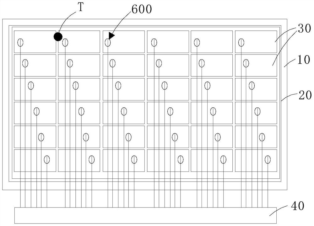
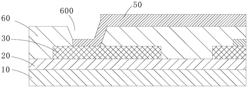
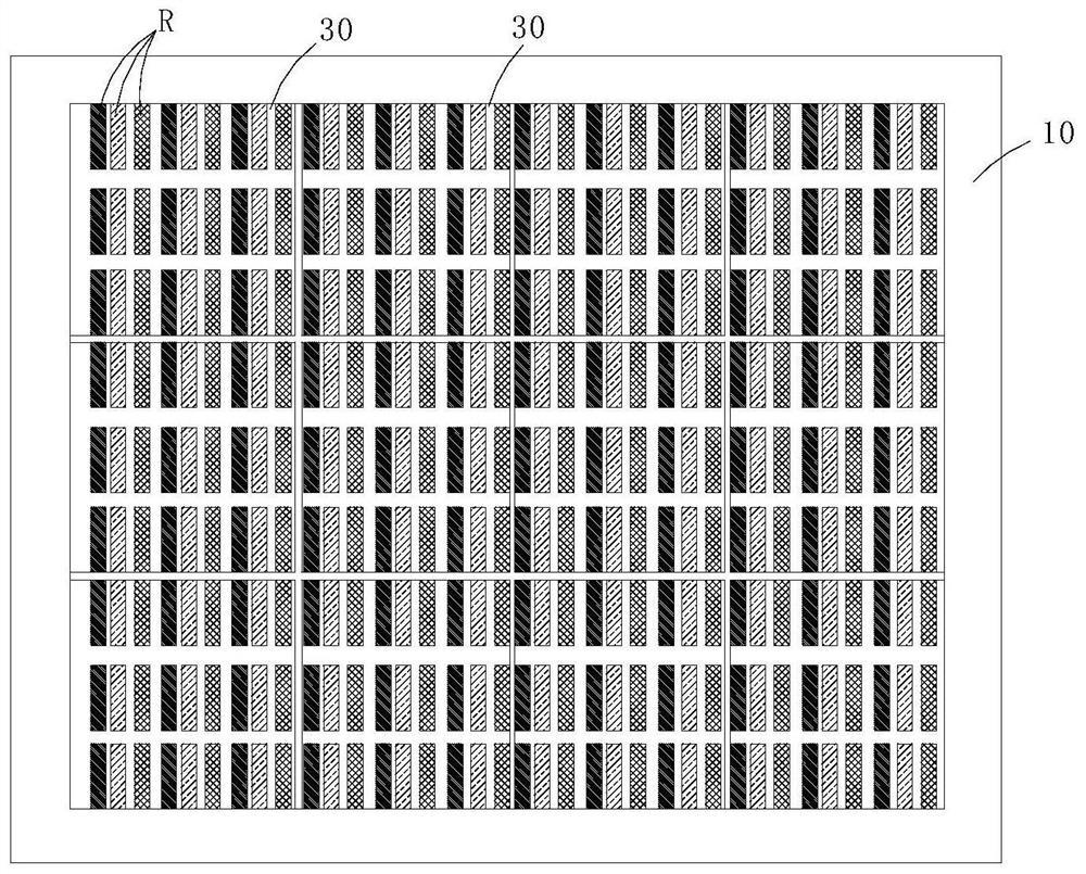
[0033]Refer tofigure 1 The active identification type liquid crystal display device of the embodiment of the present invention includes a light-transmissive first substrate 10, a light switching layer 20 covering one side surface of the first substrate 10, and two adjacently arranged at intervals on the surface of the light switching layer 20. A plurality of transparent electrodes 30 and a driving chip 40 connected to all the electrodes 30 at the same time. Every two electrodes 30 are insulated from each other. The light switching layer 20 is used to generate photo-generated current after illuminati...


PUM


Abstract

The invention discloses an active identification type liquid crystal display device and a manufacturing method thereof. The liquid crystal display device comprises a first light-penetrating substrate,an illumination switching layer, a plurality of transparent electrodes and a driving chip, wherein the surface on one side of the first substrate is covered with the illumination switching layer, thetransparent electrodes are adjacent in pairs and are alternately arranged on the surface of the illumination switching layer, the driving chip is connected with all the electrodes, and every two electrodes are insulated from each other. According to the active identification type liquid crystal display device, the illumination switching layer capable of generating photo-generated current after illumination is formed on the surface of the first substrate, when laser from a laser pen shines on the surface of the portion, at the gap of two adjacent electrodes, of the illumination switching layer, the photo-generated current is produced, so that the two adjacent electrodes are switched on, and by sensing the position of a switch-on signal, the position, directed by the beam of the laser pen,on the display device can be conveniently captured; the illumination switching layer generates the photo-generated current after illumination, deflection of liquid crystals corresponding to the area where the photo-generated current is generated is controlled by the driving chip, and active identification and pattern display of the liquid crystal display device to the beam position are achieved.

Description

Technical field[0001]The present invention relates to the field of display technology, in particular to an active recognition type liquid crystal display device and a manufacturing method thereof.Background technique[0002]In the current market, more and more large-size LCDs (Liquid Crystal Displays) are used in teaching, conference and commercial display scenes. However, due to the high reflectivity of the LCD surface, conventional laser pointers cannot be used for presentation, which affects The presenter demonstrates the convenience.[0003]In this regard, the current mainstream method is to add fog treatment on the display surface and change the reflection to diffuse reflection, but the projection brightness of the laser pointer on the display surface is still very low and it becomes blurry and difficult to distinguish, and the screen is treated with high haze. At the same time, it will reduce the display effect of the monitor. If another method is adopted, simply adding a light se...

Claims


Application Information

Patent Timeline
Patent Type & Authority Patents(China)
IPC IPC(8): G02F1/1343G02F1/1333G06F3/0481
CPCG02F1/1333G02F1/134309G06F3/04812
Inventor 李岩松
Owner HUIZHOU CHINA STAR OPTOELECTRONICS TECHNOLOGY CO LTD
Why Eureka
Try Eureka