Organic light-emitting display panel, manufacturing method thereof and organic light-emitting display device

A technology of light-emitting display and manufacturing method, which is applied in the direction of semiconductor/solid-state device manufacturing, semiconductor devices, electrical components, etc., and can solve problems such as affecting the perception, weakening the display effect of organic light-emitting display panels, and not being able to achieve independence

Inactive Publication Date: 2018-09-07
SHANGHAI TIANMA MICRO ELECTRONICS CO LTD
View PDF3 Cites 16 Cited by
  • Summary
  • Abstract
  • Description
  • Claims
  • Application Information

AI Technical Summary

Problems solved by technology

[0004] The inventors of the present application found that when using the inkjet printing technology to prepare the organic light-emitting functional layers of organic light-emitting devices, within a pixel opening, the organic light-emitting functional layers of adjacent organic light-emitting d...

Method used


Image

  • Organic light-emitting display panel, manufacturing method thereof and organic light-emitting display device
  • Organic light-emitting display panel, manufacturing method thereof and organic light-emitting display device
  • Organic light-emitting display panel, manufacturing method thereof and organic light-emitting display device

Examples


Embodiment Construction

[0050] In order to make the purpose, technical solutions and advantages of the embodiments of the present invention clearer, the technical solutions in the embodiments of the present invention will be clearly and completely described below in conjunction with the drawings in the embodiments of the present invention. Obviously, the described embodiments It is a part of embodiments of the present invention, but not all embodiments. Based on the embodiments of the present invention, all other embodiments obtained by persons of ordinary skill in the art without creative efforts fall within the protection scope of the present invention.

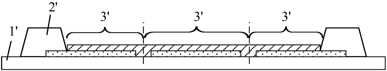
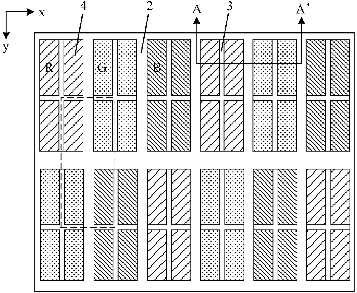
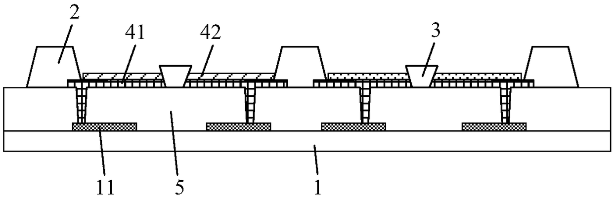
[0051] An embodiment of the present invention provides an organic light emitting display panel, such as figure 2 and image 3 as shown, figure 2 The top view of the organic light-emitting display panel provided by the embodiment of the present invention Figure 1 , image 3 Provided for the embodiment of the present invention figure 2 A sche...


PUM

PropertyMeasurementUnit
Widthaaaaaaaaaa
Thicknessaaaaaaaaaa
Thicknessaaaaaaaaaa

Abstract

The embodiment of the invention provides an organic light-emitting display panel, a manufacturing method thereof and an organic light-emitting display device, and relates to the technical field of display. The organic light-emitting display panel provided by the embodiment of the invention comprises an array substrate, a pixel definition layer, a plurality of interval structures and a plurality oforganic light-emitting devices, wherein the pixel definition layer and the interval structures are arranged on the array substrate, a plurality of pixel openings are formed in the pixel definition layer, the interval structures are used for partitioning the pixel openings into a plurality of sub-pixel openings, and the cross section of each interval structure is in the shape of a inverted trapezoid; each sub-pixel opening is internally provided with an organic light-emitting device, and the organic light-emitting devices arranged inside the same pixel opening are used for transmitting light rays with the same color; each organic light-emitting device comprises an anode and at least one organic light-emitting functional layer, and the organic light-emitting functional layers positioned ontwo sides of each internal structure are separated from each other. Through the technical scheme, the display effect of the organic light-emitting display panel can be improved.

Description

technical field [0001] The present invention relates to the field of display technology, in particular to an organic light emitting display panel, a manufacturing method thereof, and an organic light emitting display device. Background technique [0002] With the rapid development of flat panel display technology, organic light emitting display panels (Organic Light Emitting Display, OLED for short) are more and more widely used due to their excellent characteristics such as self-illumination, high brightness, wide viewing angle, and fast response. [0003] Such as figure 1 as shown, figure 1 A schematic cross-sectional view of an organic light-emitting display panel provided in the prior art. The organic light-emitting display panel includes an array substrate 1', a pixel definition layer 2' on the array substrate 1', and a plurality of organic light-emitting devices 3', wherein the pixel definition layer 2' has a plurality of pixel openings, and the organic light emittin...

Claims


Application Information

Patent Timeline
IPC IPC(8): H01L27/32H01L51/52H01L51/56
CPCH10K59/121H10K59/122H10K50/80H10K71/00
Inventor 霍思涛
Owner SHANGHAI TIANMA MICRO ELECTRONICS CO LTD
Why Eureka
Try Eureka