
A kind of photosensitive film and preparation method thereof
A photosensitive film and photosensitive layer technology, which is applied in the field of engineering plastics, can solve problems such as cracking and film deformation, and achieve the effects of strong adhesion, low cost, and high production efficiency
- Summary
- Abstract
- Description
- Claims
- Application Information
AI Technical Summary
Problems solved by technology
Method used
Image

Examples
Embodiment 1
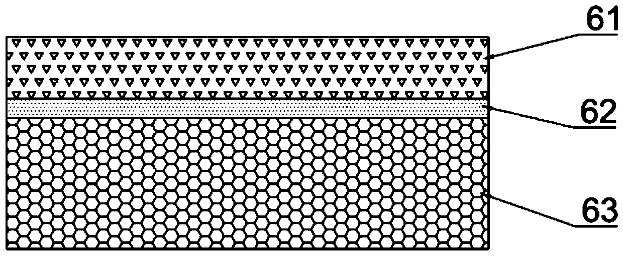
[0029] Such as figure 1 Shown, a kind of photosensitive film comprises polycarbonate PC layer 63, polymethyl methacrylate PMMA layer 61 and the photosensitive layer 62 between polycarbonate PC layer 63 and polymethyl methacrylate PMMA layer 61 The raw materials of the photosensitive layer 62 are transparent photochromic powder, nano-scale conductive antistatic agent and organic silicon compatible coupling agent with two active functional groups of methyl group and phenyl group.
[0030] In another embodiment, the thickness of the photosensitive layer 62 is 1-10 μm.
[0031] In another embodiment, the nano-scale conductive antistatic agent includes silver nanowires and / or nano-indium tin oxide.
[0032] The invention also discloses a method for preparing the photosensitive film, which includes the following steps:
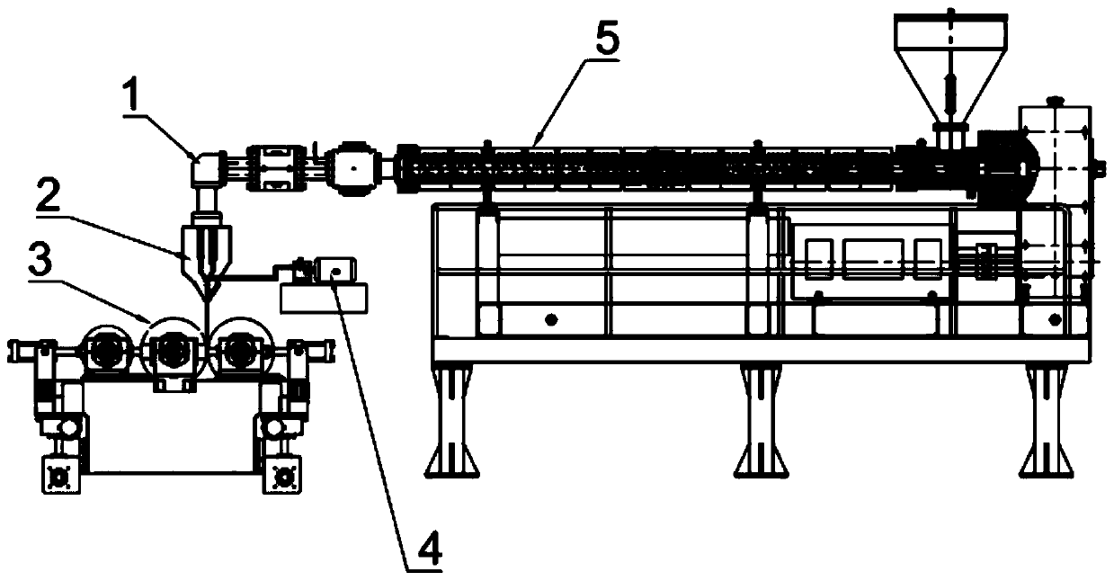
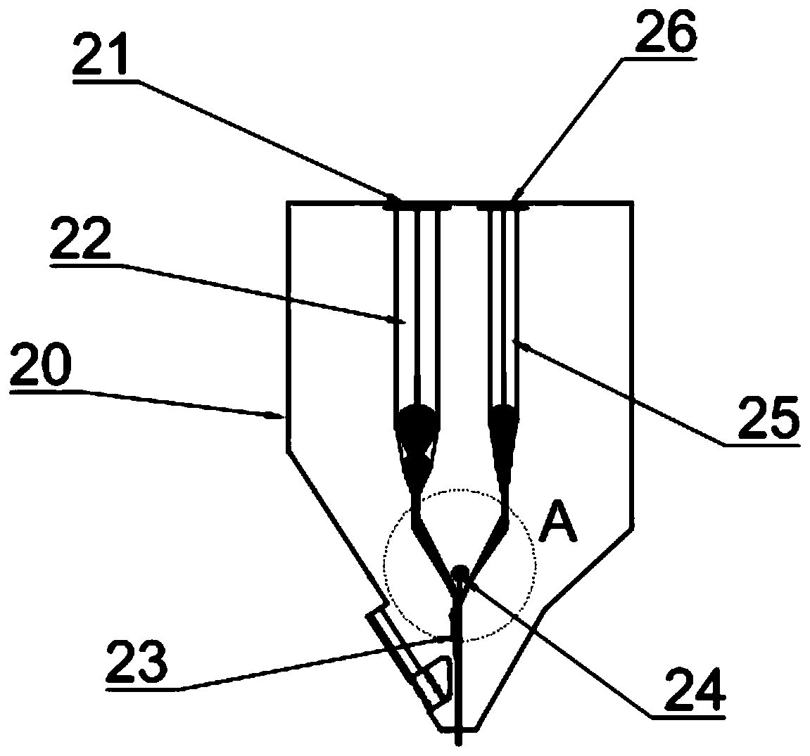
[0033] A, polycarbonate PC material and polymethyl methacrylate PMMA material are packed in two plastic extruders 5 respectively, the photosensitive layer materia...
PUM
| Property | Measurement | Unit |
|---|---|---|
| width | aaaaa | aaaaa |
| diameter | aaaaa | aaaaa |
| thickness | aaaaa | aaaaa |
Abstract
Description
Claims
Application Information