

Trench gate power MOS transistor containing semi-insulating region and preparation method
A MOS transistor and semi-insulating technology, applied in the field of trench gate power MOS transistors and their fabrication, can solve problems such as low avalanche resistance, and achieve the effects of improving breakdown voltage, ensuring threshold voltage, and improving avalanche resistance and robustness.
- Summary
- Abstract
- Description
- Claims
- Application Information
AI Technical Summary
Problems solved by technology
Method used
Image

Examples
Embodiment 1
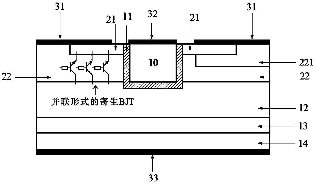
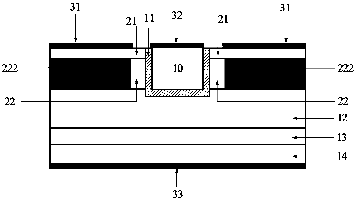
[0050] Combine image 3 , 4 A trench gate power MOS transistor with a semi-insulating region of this embodiment includes a source region 21 doped with a second conductivity type, a base region 22 doped with a first conductivity type, and a semi-insulating region 222. The second conductivity type The doped source region 21 is located above the first conductive type doped base region 22 and the semi-insulated region 222 arranged side by side, and the bottom of the semi-insulated region 222 is in contact with the second conductive type doped drift layer 12.
[0051] The existence of the semi-insulating region 222 reduces the area where parasitic BJTs exist, that is, reduces the number of parasitic BJTs, but there are a small amount of parasitic BJTs under the channel region, but the number of parasitic BJTs is greatly reduced, thereby reducing Under UIS conditions, the current in the MOSFET limits the increase in temperature. The avalanche breakdown time of the MOSFET is increased fr...
Embodiment 2
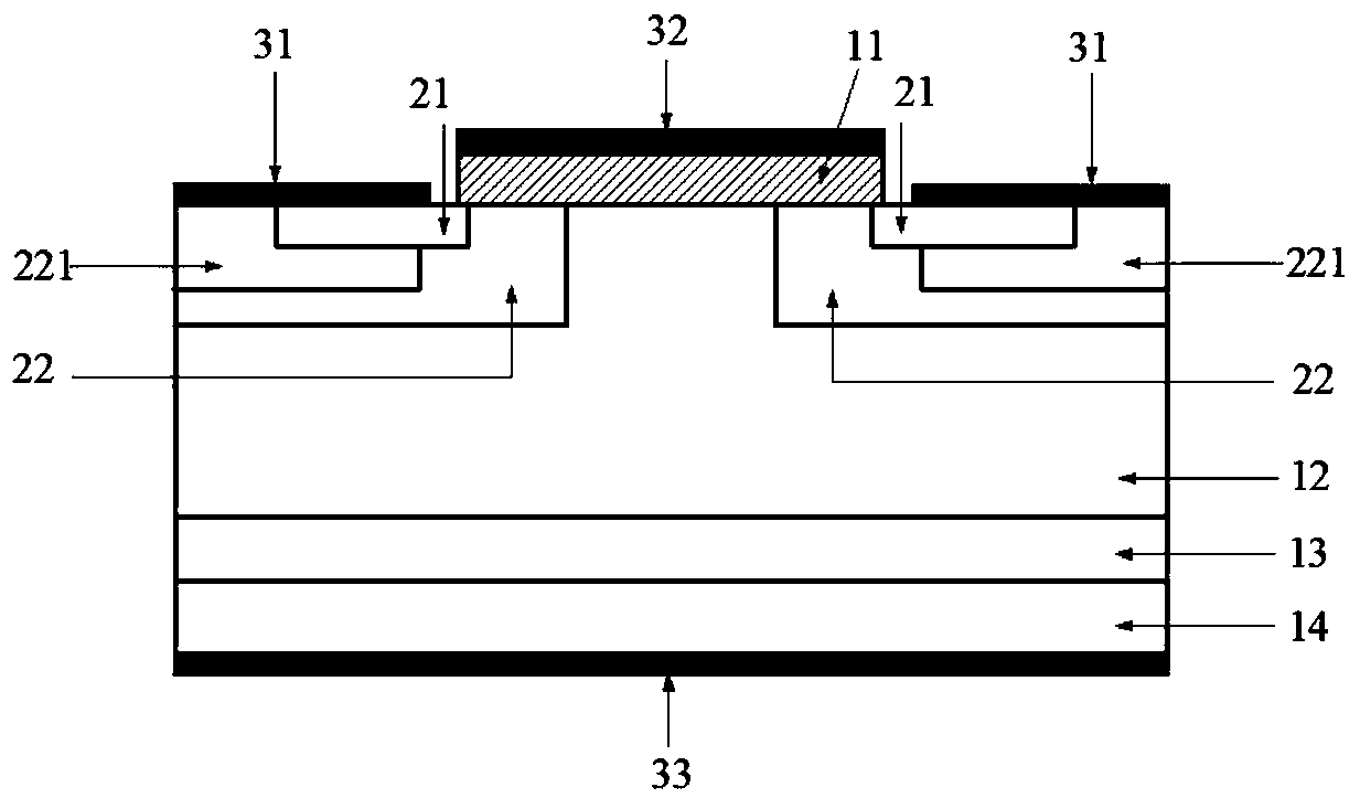
[0056] Combine image 3 , 4 , The trench gate power MOS transistor with semi-insulating region of this embodiment is further improved on the basis of embodiment 1. The width of the source region 21 doped with the second conductivity type is the same as the base region doped with the first conductivity type. The sum of the widths of 22 and the semi-insulating region 222 is equal.
[0057] Precisely control the effective width of the conductive channel formed by the doped base region 22 of the first conductivity type, without changing due to the introduction of the semi-insulating region 222, ensuring the threshold voltage, on-resistance, and transconductance of the trench gate power MOS transistor , Output characteristics and other parameters do not change due to the introduction of the semi-insulated region 222. While not affecting the channel region of the trench gate power MOS transistor, it can not only improve the avalanche tolerance and robustness of the trench gate power MO...
Embodiment 3
[0059] Combine image 3 , 4 In this embodiment, a trench gate power MOS transistor with a semi-insulating region is further improved on the basis of Embodiments 1 and 2. The depth of the base region 22 doped with the first conductivity type is the same as the depth of the semi-insulating region 222 . The width ratio of the first conductive type doped base region 22 to the second conductive type doped source region 21 is 1:1-3. For specific applications, you can choose values such as 1:1; 1:2; 1:3; 1:1.5; 1:2.8.
[0060] Ensure that the effective channel length of the trench-gate power MOS transistor does not change due to the introduction of the semi-insulated region 222, and ensure that the threshold voltage, on-resistance, transconductance, and output characteristics of the trench-gate power MOS transistor are not affected by the semi-insulated region. Introduced and changed. Ensure that the channel carriers are transported smoothly and there is no "overstep", otherwise the...
PUM
 Abstract
Description
Claims
Application Information