Full-surface display screen and display device adopting same

A technology of display device and display screen, applied in static indicators, optics, instruments, etc., can solve problems such as box lighting test and timing, flexible circuit board yield reduction, size reduction and other problems affecting liquid crystal panels

Pending Publication Date: 2018-11-20
WUHAN CHINA STAR OPTOELECTRONICS TECH CO LTD
View PDF8 Cites 17 Cited by
  • Summary
  • Abstract
  • Description
  • Claims
  • Application Information

AI Technical Summary

Problems solved by technology

[0006] (1) After the lower border continues to narrow, the yield rate of chip bonding (Bonding) to the flexible circuit board decreases;
[0007] (2) In the COF packaging process, when the width of the lower frame is 1.8mm or 1.6mm, the size of the cell test pad on the LCD panel is greatly reduced, which affects the cell test and timing of the LCD panel ( Timing) debugging
[0008] (3) Whether the width of the bottom frame is 1.8mm or the width of the bottom frame is 1.6mm, it is impossible to achieve the state of no bottom frame similar to Iphone X, and there will always be a "chin".
Existing notch full display COF panel designs cannot meet the above requirements and a new full display design needs to be invented

Method used


Image

  • Full-surface display screen and display device adopting same
  • Full-surface display screen and display device adopting same
  • Full-surface display screen and display device adopting same

Examples


Embodiment Construction

[0027] The full display screen provided by the present invention and the specific implementation of the display device using the full display screen will be described in detail below in conjunction with the accompanying drawings.

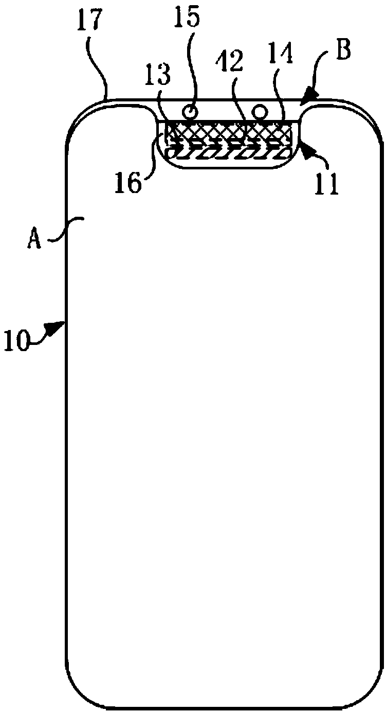
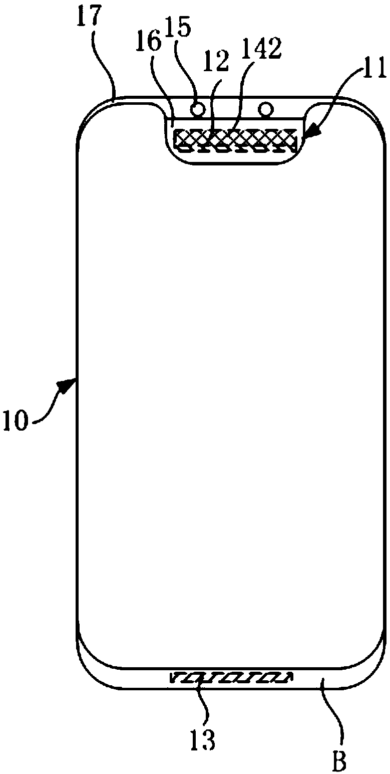
[0028] figure 1 It is a top view structure diagram of the first embodiment of the comprehensive display screen of the present invention, please refer to figure 1 , the comprehensive display screen 1 of the present invention includes a display unit 10 . The display unit 10 includes a display area A and a non-display area B. Wherein, the non-display area B may surround the display area A, or may be only arranged above and / or below the display area A.

[0029] There is a notch 11 at the upper end of the display area A, and the notch 11 is located in the non-display area B, that is, no picture is displayed at the notch 11 . In this embodiment, the position where the notch 11 is located is the non-display area B, and the other areas of the display uni...


PUM


Abstract

The invention provides a full-surface display screen and a display device adopting the same. The full-surface display screen comprises a display unit, the display unit comprises a display region and anon-display region, a notch is formed in the upper end of the display unit and located in the non-display region, the full-surface display screen further comprises a chip-on-film binding welding padand a cell testing welding pad, the chip-on-film binding welding pad and the cell test welding pad are arranged on the non-display region, and at least one of the chip-on-film binding welding pad andthe cell test welding pad is arranged in the notch. The full-surface display screen has the advantages that at least one of the chip-on-film binding welding pad and the cell test welding pad is arranged in the notch, a lower border is super narrow, and even no border exists. Meanwhile, the requirements for cell light-on testing of the super-narrow lower border and the yield of chip-on-film bindingof the full-surface display screen can be met.

Description

technical field [0001] The invention relates to the field of liquid crystal displays, in particular to a full display screen and a display device using the full display screen. Background technique [0002] At present, the popularity of full-screen mobile phones is getting higher and higher, and screens with high screen-to-body ratios are becoming more and more popular. As a result, many narrow bezel solutions have been created, mainly for the left and right bezels, but for mobile phones, the lower bezels have always been improved to increase the screen-to-body ratio. It's a big issue. The so-called screen-to-body ratio is the ratio of the screen area to the overall machine area. A higher screen-to-body ratio can bring users a better visual experience. Due to its high screen-to-body ratio and good display effect, the full-screen display has become more and more popular among consumers and has become an inevitable trend in the future development of electronic devices such as...

Claims


Application Information

Patent Timeline
Patent Type & Authority Applications(China)
IPC IPC(8): G02F1/1333G02F1/133G02F1/1335
CPCG02F1/133G02F1/1333G02F1/133308G02F1/133512G02F1/133331H05K2201/10136H05K1/148H05K2201/10681H05K1/0268G02F1/13452G02F1/1309G02F1/13458H05K1/189
Inventor 杨思捷
Owner WUHAN CHINA STAR OPTOELECTRONICS TECH CO LTD
Why Eureka
Try Eureka