Method of producing ultra-thin copper foil with carrier, ultra-thin copper foil with carrier produced by the same, printed circuit board, multilayer printed circuit board and chip on film circuit board

a technology of carrier and ultra-thin copper, which is applied in the direction of solid-state devices, metal-working apparatus, metal-patterned materials, etc., can solve the problems of nearly 0 surface roughness of rz of 0.01 m, uneven roughness of films,

Inactive Publication Date: 2007-05-29
FURUKAWA ELECTRIC CO LTD
View PDF10 Cites 20 Cited by
  • Summary
  • Abstract
  • Description
  • Claims
  • Application Information

AI Technical Summary

Benefits of technology

[0017]In view of the above-mentioned circumstances, an object of the present invention is, in order to produce an ultra-thin copper foil with a carrier having few pinholes and small surface roughness as for an ultra-thin copper foil of 5 μm or less without changing the current cost of production manufacturing and produce a production satisfying user's way, to provide an ultra-thin copper foil with a carrier having few pinholes and small surface roughness and the producing method by using a carrier foil that is made smooth surface of a carrier foil which is an electrodeposited or a rolled copper or a copper alloy at the process such as the mechanical polishing, the chemical polishing, the electrochemical polishing, or the smoothing plating processing method independently, or combining two or more, and to produce a printed circuit board for fine pattern, a multilayer printed circuit board and a chip on film circuit board.

Problems solved by technology

For example, in the case that this ultra-thin copper foil is used for COF mounting, unevenness of the films is roughened because the surface unevenness of a copper foil is printed at forming a circuit pattern with an ultra-thin copper foil, as a consequence transmittance is nearly 0.
Moreover, since a surface roughness of Rz of 0.01 μm or less is impractical because of being difficult to produce a foil stably from the view of technique and being expensive, it is preferable that the mean surface roughness is set to Rz of 0.01 to 2.0 μm.

Method used


Image

  • Method of producing ultra-thin copper foil with carrier, ultra-thin copper foil with carrier produced by the same, printed circuit board, multilayer printed circuit board and chip on film circuit board
  • Method of producing ultra-thin copper foil with carrier, ultra-thin copper foil with carrier produced by the same, printed circuit board, multilayer printed circuit board and chip on film circuit board

Examples


example 1

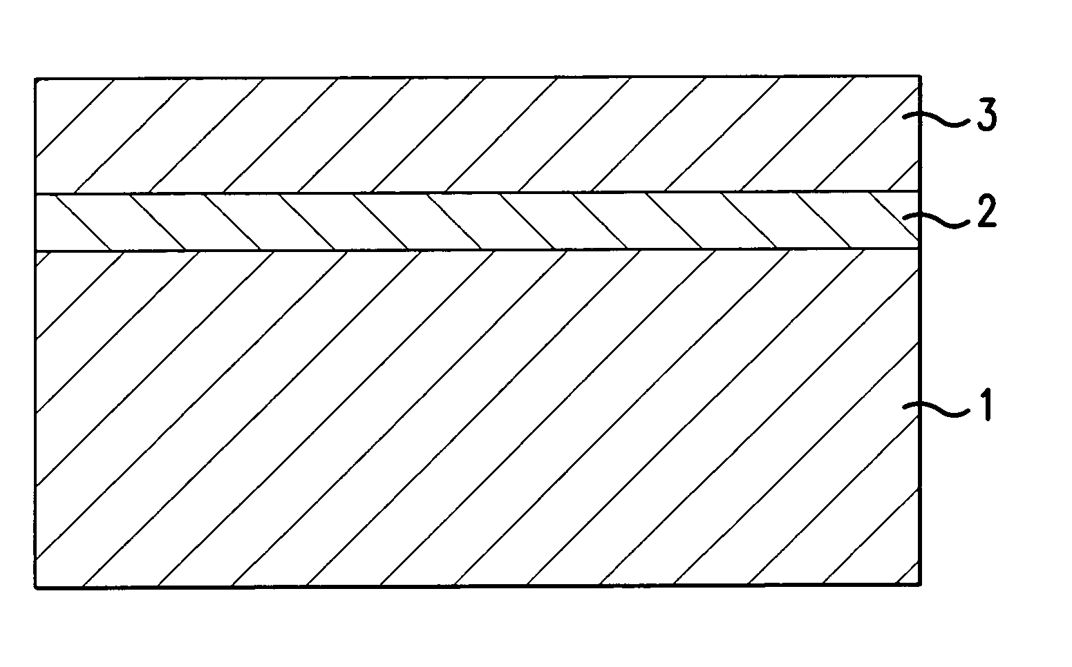
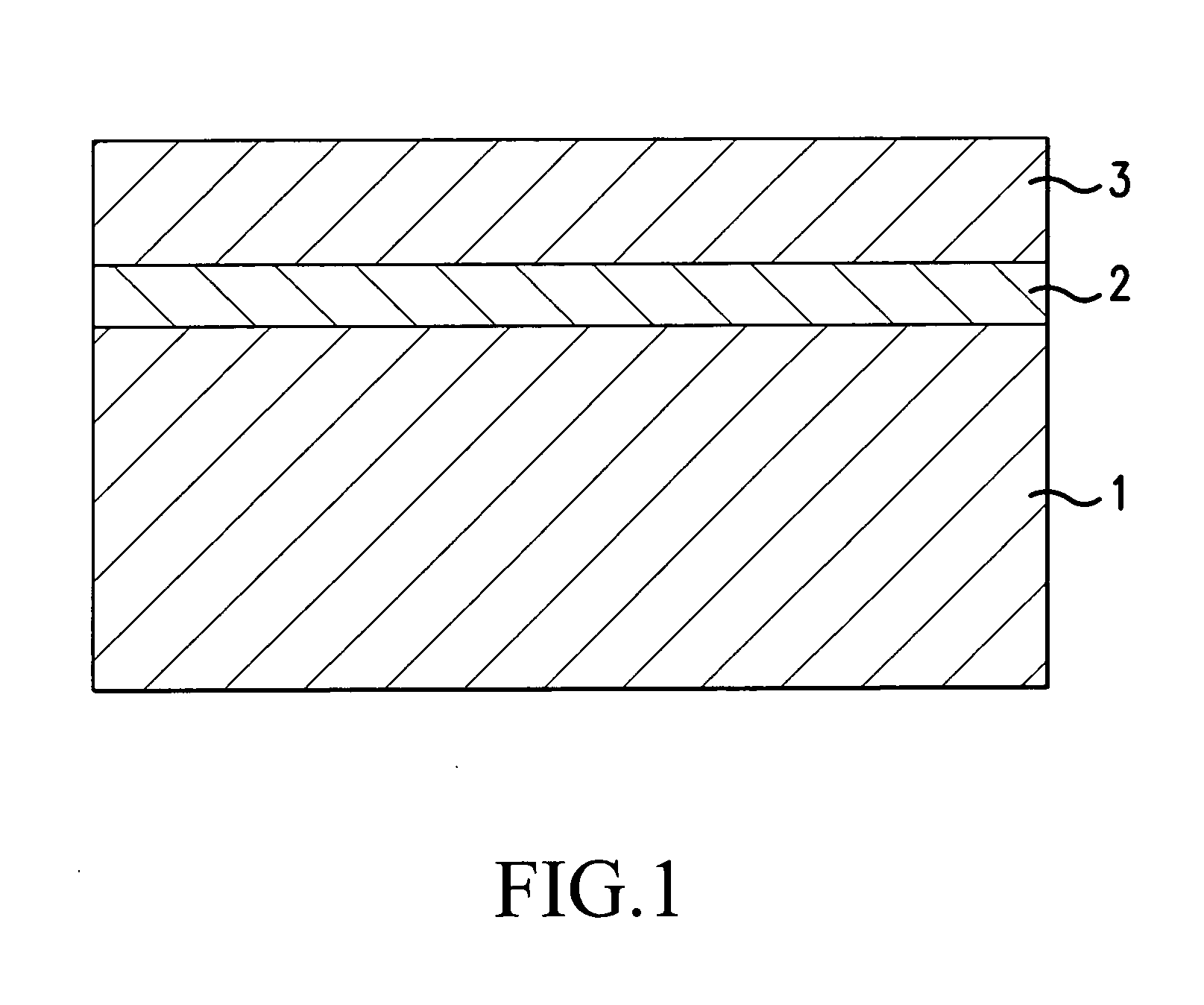
[0060]1. Smoothing of Carrier Foil

[0061]An electrodeposited copper foil having a surface roughness Rz of 2.1 μm and a thickness of 35 μm was made into an anode and in an electrolytic solution of the sulfuric concentration of 50 g / l, passing the current having the current density of 25 A / dm2 for 20 seconds made the surface smooth by dissolving, and the smoothed surface having Rz of 0.65 μm was obtained. The electrodeposited copper foil having this smoothed surface was made as a carrier copper foil.

[0062]2. Formation of Peeling Layer

[0063]Electroplating of chromium was continuously performed on the smoothed surface of a carrier copper foil being made smooth, and the chromium plating peeling layer of the amount of deposition of 0.50 mg / dm2 was formed. In this surface layer the hydrated oxide film was formed.

[0064]3. Formation of Ultra-Thin Copper Foil

[0065]Next, on this chromium plating peeling layer the ultra-thin copper foil was plated by using the following plating bath in the elect...

example 2

[0068]1. Smoothing of Carrier Foil

[0069]After performing the mechanical polishing of the copper foil having Rz of 1.7 μm and the thickness of 55 μm and smoothing the mean surface roughness of Rz to 1.2 μm, this foil was made into an anode, in the electrolytic solution of the pyrophosphoric acid of concentration of 100 g / l, passing the current having the current density of 22 A / dm2 for 50 seconds made the surface smooth by dissolving, and the smoothed surface copper foil (carrier copper foil) having Rz of 0.55 μm was obtained.

[0070]2. Formation of Peeling Layer

[0071]Electroplating of chromium was continuously performed on the smoothed surface of a carrier copper foil being made smooth, and the chromium plating peeling layer of the amount of deposition of 0.50 mg / dm2 was formed. In this surface layer the hydrated oxide film was formed.

[0072]3. Formation of Ultra-Thin Copper Foil

[0073]On this chromium plating peeling layer, a copper strike-plating was performed for 30 seconds under the...

example 3

[0078]1. Smoothing of Carrier Foil

[0079]Electrodeposited copper foil having Rz of 1.5 μm and the thickness of 35 μm was made immersed for 120 seconds in the solution containing sulfuric acid of the concentration of 100 g / l and hydrogen peroxide solution of 5%, it made smooth, and the smoothed surface of Rz of 1.2 μm was obtained. An electrodeposited copper foil having this smoothed surface was made as a carrier copper foil.

[0080]2. Formation of Peeling Layer

[0081]Electroplating of nickel-molybdenum was continuously performed on the smoothed surface of a carrier copper foil being made smooth, and nickel-molybdenum plating layer of the deposited amount 0.3 mg / dm2 was formed.

[0082]3. Formation of Ultra-Thin Copper Foil

[0083]Next, on the nickel-molybdenum peeling layer, an ultra-thin copper foil with a carrier was plated by using the following plating bath in the electric current density 5 A / dm2, and the ultra-thin copper foil was to be the thickness of 5 μm.

[0084]

Cu2P2O7.3H2O: 85 g / lK4...


PUM

PropertyMeasurementUnit
surface roughness Rzaaaaaaaaaa
mean surface roughness Rzaaaaaaaaaa

Abstract

An object of the present invention is to produce an ultra-thin copper foil with a carrier which has few pinholes and small surface roughness and which has an the thickness of less than 5 μm, and to produce the method of producing the foil, and further to produce a printed circuit board for fine pattern, a multilayer printed circuit board and a chip on film circuit board by using the ultra-thin copper foil with a carrier. The present invention provides an ultra-thin copper foil with a carrier produced by stacking a peeling layer and an ultra thin copper foil in order on the surface of a carrier copper foil which is made smooth so that the mean surface roughness of at least one side is Rz of 0.01 to 2.0 μm by the chemical polishing, the electrochemical dissolution, or the smoothing plating processing method independently, combining two or more, or further combining the mechanical polishing.

Description

BACKGROUND OF THE INVENTION[0001]1. Field of the Invention[0002]The present invention relates to a method of producing an ultra-thin copper foil with a carrier and an ultra-thin copper foil with a carrier produced by the same, in particular, to an ultra-thin copper foil with a carrier suitable for a printed circuit board for high density ultra-fine circuit applications (fine pattern), a multilayer printed circuit board and a chip on film circuit board.[0003]2. Description of the Related Art[0004]A printed circuit board is produced as follows.[0005]First, a thin foil for forming a surface circuit is put on an electrically insulating board comprised of a glass-epoxy resin, a glass polyimide resin, etc., and then they are heated and pressed to produce a copper-cladding laminate board.[0006]Next, this copper-cladding laminate board is successively formed with the through holes and plated at the through holes, then the copper foil at the surface of the copper-cladding laminate board is e...

Claims


Application Information

Patent Timeline
Patent Type & Authority Patents(United States)
IPC IPC(8): B32B15/00H05K1/09B32B15/20C25D1/04C25D7/00C25D7/06H05K3/02H05K3/38H05K3/46
CPCC25D1/04H05K3/384H05K3/025Y10T428/12028H05K2201/0355H05K2201/0723H01L2924/0002Y10T428/12514Y10T428/12493Y10T428/12472Y10T428/12535Y10T428/12806Y10T428/12778H01L2924/00H05K3/38
Inventor SUZUKI, YUUJIMATSUDA, AKIRA
Owner FURUKAWA ELECTRIC CO LTD
Why Eureka
Try Eureka