Relief type diffraction optical element, optical system comprising the same and mold for manufacturing the same
- Summary
- Abstract
- Description
- Claims
- Application Information
AI Technical Summary
Benefits of technology
Problems solved by technology
Method used
Image
Examples
second embodiment
FIG. 9 is a schematic cross sectional view showing the relief type diffraction grating according to the invention. In the present embodiment, use is made of a substrate having a plane-convex shape and the non-even width relief type diffraction grating pattern is formed in a convex surface. In the present embodiment, a necessary power of the lens is obtained by a combination of the refractive spherical surface and the non-even width diffraction pattern, it is possible to widen pitches of the diffraction pattern. Therefore, by forming only the central zone to have the ideal curvilinear cross sectional configuration, the intensity of light converged at the focal point can be increased. Also in this case, the non-even width diffraction grating pattern may be also formed on the plane surface of the substrate.
In the above embodiments, only the central zone having the maximum width or pitch is formed to have the ideal curvilinear cross sectional configuration following the phase shift func...
fifth embodiment
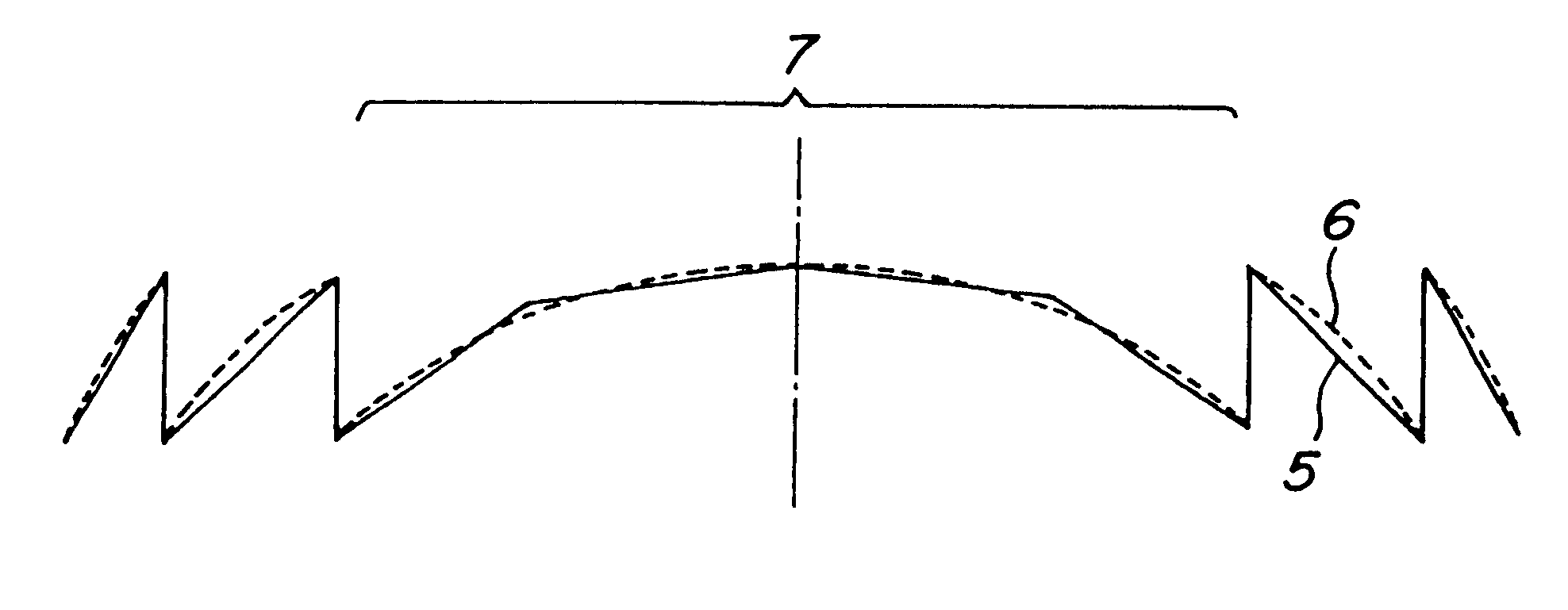
FIG. 16 is a schematic cross sectional view showing the relief type diffraction grating according to the invention. In the present embodiment, use is made of a substrate having a plane-convex shape and the non-even width relief type diffraction grating pattern is formed in a convex surface. The central zone of the diffraction type lens of the present embodiment is formed to have a cross sectional configuration composed of two rectilinear portions. In the present embodiment, it is possible to widen pitches of the diffraction pattern, and thus it is very effective to form only the central zone to have a cross sectional configuration composed of the two portions in order to increase an intensity of light converged at the focal point. Also in this case, the non-even width diffraction grating pattern may be formed in the both major surfaces of the substrate.
In the above embodiments shown in FIGS. 12, 15 and 16, only the central zone having the maximum width or pitch is formed to have the...
PUM
 Abstract
Description
Claims
Application Information


