Semiconductor device with alternating conductivity type layer and method of manufacturing the same

Inactive Publication Date: 2005-02-17
FUJI ELECTRIC CO LTD
View PDF5 Cites 36 Cited by
  • Summary
  • Abstract
  • Description
  • Claims
  • Application Information

AI Technical Summary

Benefits of technology

[0028] According to another aspect of the invention, the first buried regions and the second buried regions are formed by diffusing respective impurities into a highly resistive layer laminate epitaxially grown on the layer with low electrical resistance. By the above described manufacturing method, the semiconductor device with an alternating conductivity type laye

Problems solved by technology

Highly resistive n−-type drift layer 12 is depleted when the MOSFET is in the OFF-state, resulting in a high breakdown voltage of the MOSFET.
However, when using conventional epitaxial growth techniques, it is difficult to bury a good quality semiconductor layer in such a narrow and deep trench (with a large aspect ratio).
However, it is difficult to employ the

Method used


Image

  • Semiconductor device with alternating conductivity type layer and method of manufacturing the same
  • Semiconductor device with alternating conductivity type layer and method of manufacturing the same
  • Semiconductor device with alternating conductivity type layer and method of manufacturing the same

Examples


Example

First Embodiment

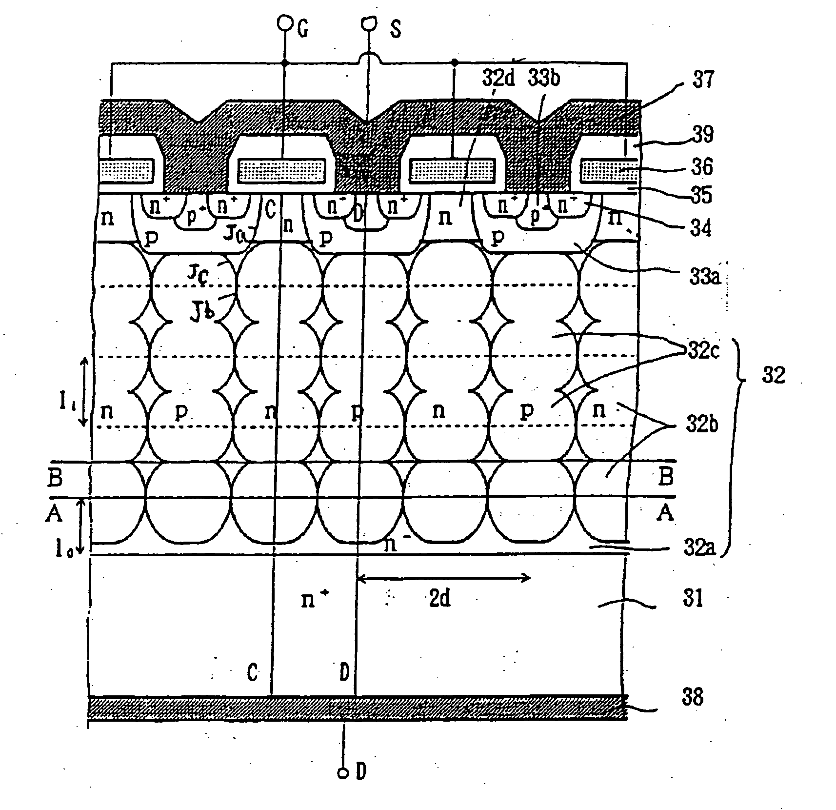
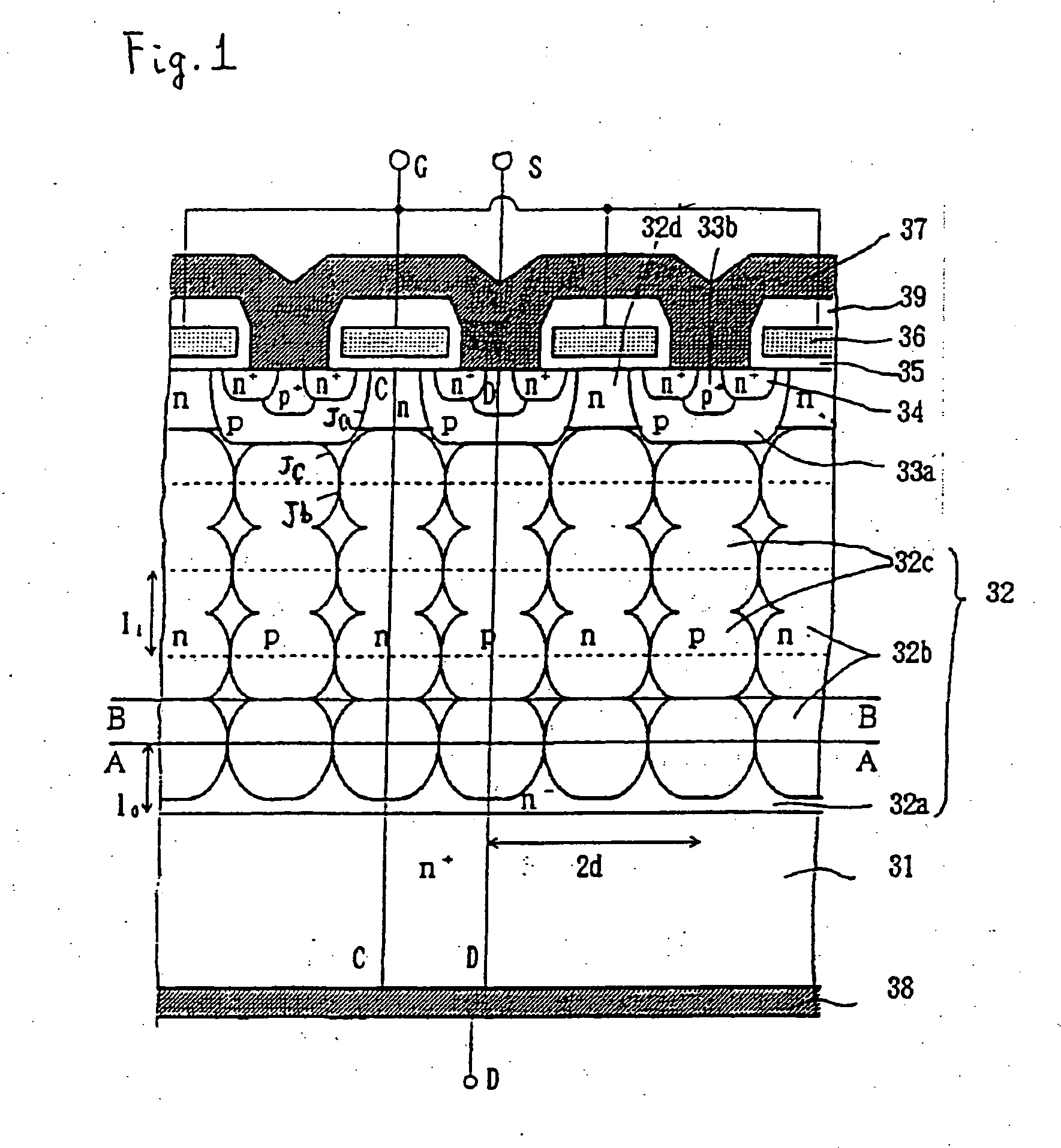
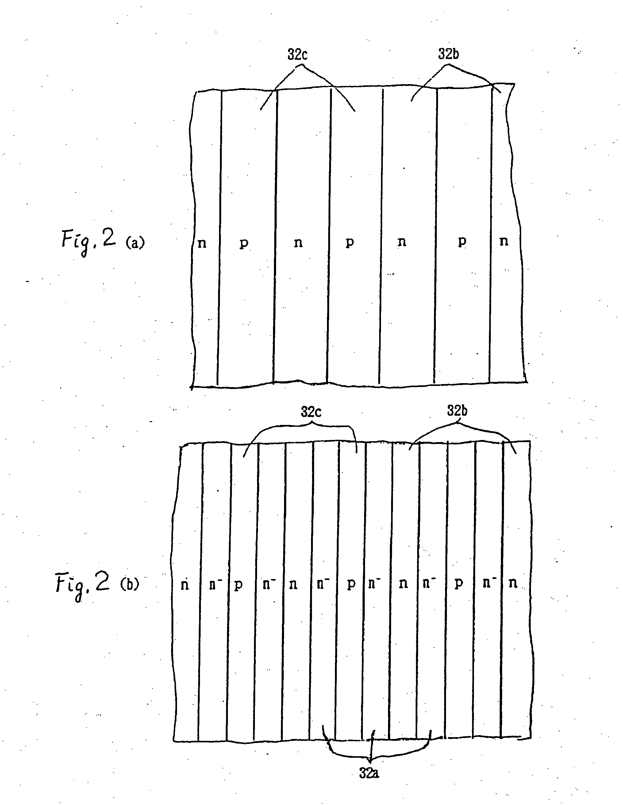
[0053]FIG. 1 is a cross section of a semiconductor device with an alternating conductivity type layer according to a first embodiment of the invention. FIG. 2(a) is a cross section along A-A of the semiconductor device with an alternating conductivity type layer of FIG. 1. FIG. 2(b) is a cross section along B-B of the semiconductor device with an alternating conductivity type layer of FIG. 1.

[0054] Referring now to FIG. 1, a semiconductive substrate region 32 is formed on an n+-type, low resistance, drain layer 31. Semiconductive substrate region 32 includes a highly resistive n−-type layer 32a, a plurality of vertical alignments of n-type buried regions 32b and a plurality of vertical alignments of p-type buried regions 32c. The vertical alignments of n-type buried regions 32b and the vertical alignments of p-type buried regions 32c are alternately arranged with each other horizontally. An n-type channel layer 32d is in contact with the uppermost n-type buried reg...

Example

Second Embodiment

[0081]FIG. 13 is a cross section of a semiconductor device with alternating conductivity type layer according to a second embodiment of the invention.

[0082] Referring now to FIG. 13, a drift layer 42 is on an n+-type drain layer 41 with low resistance. Drift layer 42 includes a highly resistive layer 42a, a plurality of vertical alignments of n-type buried regions 42b and a plurality of vertical alignments of p-type buried regions 42c. The vertical alignments of n-type buried regions 42b and the vertical alignments of p-type buried regions 42c are alternately arranged with each other horizontally. In the surface portion of drift layer 42, n-type channel layers 42d are formed on the uppermost n-type buried regions 42b and p-type base regions 43a on the uppermost p-type buried regions 42c. An n+-type source region 44 and a heavily doped p+-type well region 43b are in p-type base region 43a. A gate electrode layer 46 is above the extended portion of p-type base regio...

Example

Third Embodiment

[0087]FIG. 14 is a cross section of a semiconductor device with an alternating conductivity type layer according to a third embodiment of the invention.

[0088] The semiconductor device shown in FIG. 14 is a UMOSFET that includes trench gates. The gate structure of the UMOSFET is different from that of the MOSFET according to the first embodiment. Referring now to FIG. 14, trenches are dug in the surface portion of a drift layer 52. A gate electrode layer 56 is surrounded by a gate insulation film 55 in the trench. In the remaining surface portion of drift layer 52, p-type base layers 53a are formed in the depth as shallow as that of gate electrode layer 56, and n+ source regions 54 are formed along the upper edges of gate electrode layers 56. A thick insulation film 59 covers gate electrode layers 56. Drift layer 52 includes a plurality of vertical alignments of n-type buried regions 52b and a plurality of vertical alignments of p-type buried regions 52c, in a simil...


PUM


Abstract

A semiconductor device having an alternating conductivity type layer improves the tradeoff between the on-resistance and the breakdown voltage and facilitates increasing the current capacity by reducing the on-resistance while maintaining a high breakdown voltage. The semiconductor device includes a semiconductive substrate region, through which a current flows in the ON-state of the device and that is depleted in the OFF-state. The semiconductive substrate region includes a plurality of vertical alignments of n-type buried regions 32 and a plurality of vertical alignments of p-type buried regions. The vertically aligned n-type buried regions and the vertically aligned p-type buried regions are alternately arranged horizontally. The n-type buried regions and p-type buried regions are formed by diffusing respective impurities into highly resistive n-type layers 32a laminated one by one epitaxially.

Description

FIELD OF THE INVENTION [0001] The present invention relates to a vertical semiconductor structure that facilitates realizing both a high breakdown voltage and a high current capacity in insulated gate field effect transistors (MOSFET's), insulated gate bipolar transistors (IGBT's), bipolar transistors, diodes and such semiconductor devices. The present invention also relates to a method of manufacturing the semiconductor device with such a vertical semiconductor structure. BACKGROUND OF THE INVENTION [0002] Semiconductor devices may be roughly classified as lateral semiconductor devices wherein electrodes are arranged on a major surface and vertical semiconductor devices wherein electrodes are distributed on both major surfaces opposing each other. When the vertical semiconductor device is ON, a drift current flows in the expansion direction of a drift layer, which becomes depleted by the reverse bias voltage when the vertical semiconductor device is OFF. FIG. 19 is a cross section ...

Claims


Application Information

Patent Timeline
IPC IPC(8): H01L21/331H01L21/336H01L29/06H01L29/739H01L29/78H01L29/861H01L29/872
CPCH01L29/0619H01L29/0634H01L29/66333H01L29/66712H01L29/872H01L29/7802H01L29/7813H01L29/861H01L29/7395H01L29/0878
Inventor FUJIHIRA, TATSUHIKO
Owner FUJI ELECTRIC CO LTD
Why Eureka
Try Eureka