Chip on film packaging structure and chip on film packaging method

A chip-on-chip film and packaging structure technology, which is applied in the direction of electrical components, electrical solid devices, circuits, etc., can solve the problems of driving IC yield and reliability, and achieve the effect of increasing the folding resistance

Active Publication Date: 2010-01-13
RAYDIUM SEMICON
View PDF0 Cites 21 Cited by
  • Summary
  • Abstract
  • Description
  • Claims
  • Application Information

AI Technical Summary

Problems solved by technology

The above situation will have a serious impact on the yield and reliability of the driver IC

Method used


Image

  • Chip on film packaging structure and chip on film packaging method
  • Chip on film packaging structure and chip on film packaging method
  • Chip on film packaging structure and chip on film packaging method

Examples


Embodiment Construction

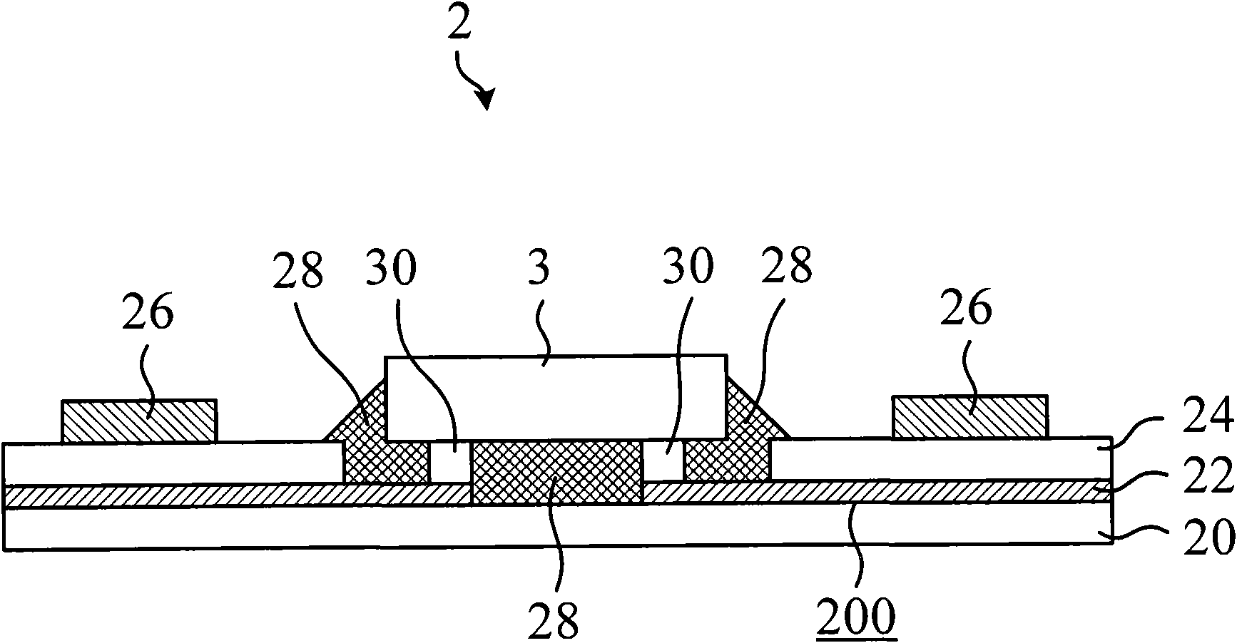
[0039] see figure 2 , figure 2 A schematic diagram of a chip-on-film packaging structure 2 according to a specific embodiment of the present invention is shown. Such as figure 2 As shown, the chip-on-film packaging structure 2 is used to package the chip 3 on the flexible substrate 20 , and the chip-on-film packaging structure 2 includes the flexible substrate 20 , the wiring layer 22 , the insulating layer 24 and the elastic layer 26 .

[0040] In this specific embodiment, the wire layer 22 may be disposed on the surface 200 of the flexible substrate 20 and includes a plurality of wires. Please note that the wire layer 22 may be composed of multiple wires in practical applications, and is not limited to its layered structure. The reason why the word "layer" is used for the wire layer 22 in this specific embodiment is to facilitate the explanation of the icon. The non-limiting wiring layer 22 is a layered structure. In addition, the insulating layer 24 is formed on the wir...


PUM


Abstract

The invention discloses a chip on film packaging structure, which comprises a flexible substrate, a lead layer, an insulating layer and an elastic layer. The flexible substrate has a surface; the lead layer is formed on the surface and is provided with a plurality of leads; the insulating layer is formed on the lead layer; and the elastic layer is formed on the insulating layer and corresponds to at least one of the leads. When the flexible substrate is bent under the action of an external force, the elastic layer can buffer the deformation of the corresponding lead. Therefore, the rupture, caused by over deformation, of the corresponding lead can be avoided. The invention also provides a chip on film packaging method, which can improve the folding endurance of the chip on film packaging structure so as to solve the problem of the prior art.

Description

technical field [0001] The present invention relates to a chip-on-film packaging structure and a chip-on-film packaging method, and in particular, the present invention relates to a chip-on-film packaging structure that can increase the folding endurance and a chip-on-film packaging that completes the chip-on-film packaging structure method. Background technique [0002] As electronic products continue to develop toward miniaturization, high speed, and high pin count, IC packaging technology is also evolving in this direction, and driver ICs on liquid crystal displays (Liquid Crystal Display, LCD) are no exception. Among them, the chip-on-chip packaging process can provide the above functions and can be used for flexible circuit boards, and is suitable for driving IC packaging of liquid crystal displays. [0003] Flip-chip packaging technology generally refers to flipping the chip and bonding it to the substrate through the metal conductor in a face-down manner. When appli...

Claims


Application Information

Patent Timeline
Patent Type & Authority Applications(China)
IPC IPC(8): H01L23/498H01L21/48
CPCH01L2224/16225H01L2224/32225H01L2224/73204H01L2924/00
Inventor 徐嘉宏王威周忠诚陈进勇
Owner RAYDIUM SEMICON
Why Eureka
Try Eureka