Voltage drop compensation method, device thereof and display device

A compensation method and technology for a compensation device, which are applied to static indicators, instruments, etc., can solve the problems of the adverse effect of the display effect of the AMOLED display device, the uneven display brightness of the AMOLED display device, and the different voltage signals, etc., and achieve long-range uniform display, Improve the display effect and compensate the effect of high precision

Active Publication Date: 2018-11-23
BOE TECH GRP CO LTD
View PDF5 Cites 29 Cited by
  • Summary
  • Abstract
  • Description
  • Claims
  • Application Information

AI Technical Summary

Problems solved by technology

However, for AMOLED display devices with large panel size and high resolution, when using the same power supply voltage (V DD ) when supplying power to each pixel unit in its display area, since the wires that transmit electrical signals corresponding to each pixel unit have different resistances, it is easy to make the same V DD After the signal is transmitted through each wire, there are different levels of voltage drop (IR Drop), which causes the actual voltage signal obtained by each pixel unit to be different. Therefore, when the same data signal (V data ) when each pixel unit is displayed and driven, each pixel unit tends to exhibit different brightness due to the existence of different IR Drops, which leads to uneven display brightness of the AMOLED display device and adversely affects the display effect of the AMOLED display device

Method used


Image

  • Voltage drop compensation method, device thereof and display device
  • Voltage drop compensation method, device thereof and display device
  • Voltage drop compensation method, device thereof and display device

Examples


Embodiment Construction

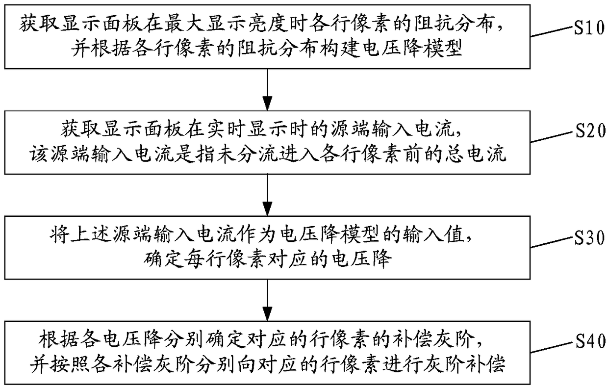
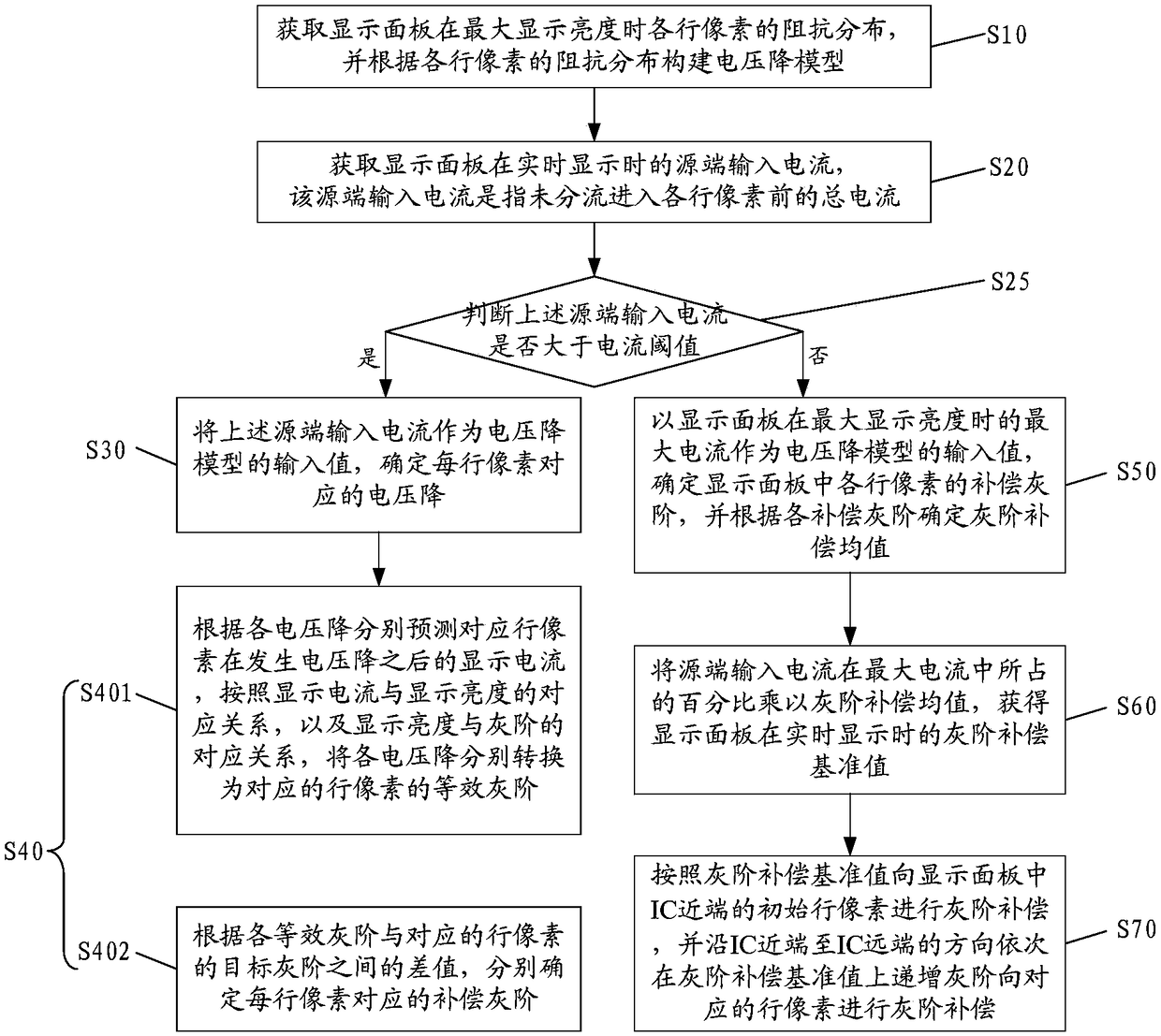
[0028] In order to further illustrate the voltage drop compensation method, its device, and the display device provided by the embodiments of the present invention, a detailed description will be given below in conjunction with the accompanying drawings.

[0029] With the continuous improvement of display panel size and display resolution in AMOLED display devices, the compensation methods commonly used in related technologies, including external optical mura compensation for TFT characteristics, and compensation circuits inside the pixel circuit, are difficult to effectively compensate for AMOLED. The voltage drop (IR Drop) caused by the increasing size of the display panel of the display device makes the AMOLED display device prone to display unevenness. Therefore, an embodiment of the present invention provides a voltage drop compensation method for solving the above problems.

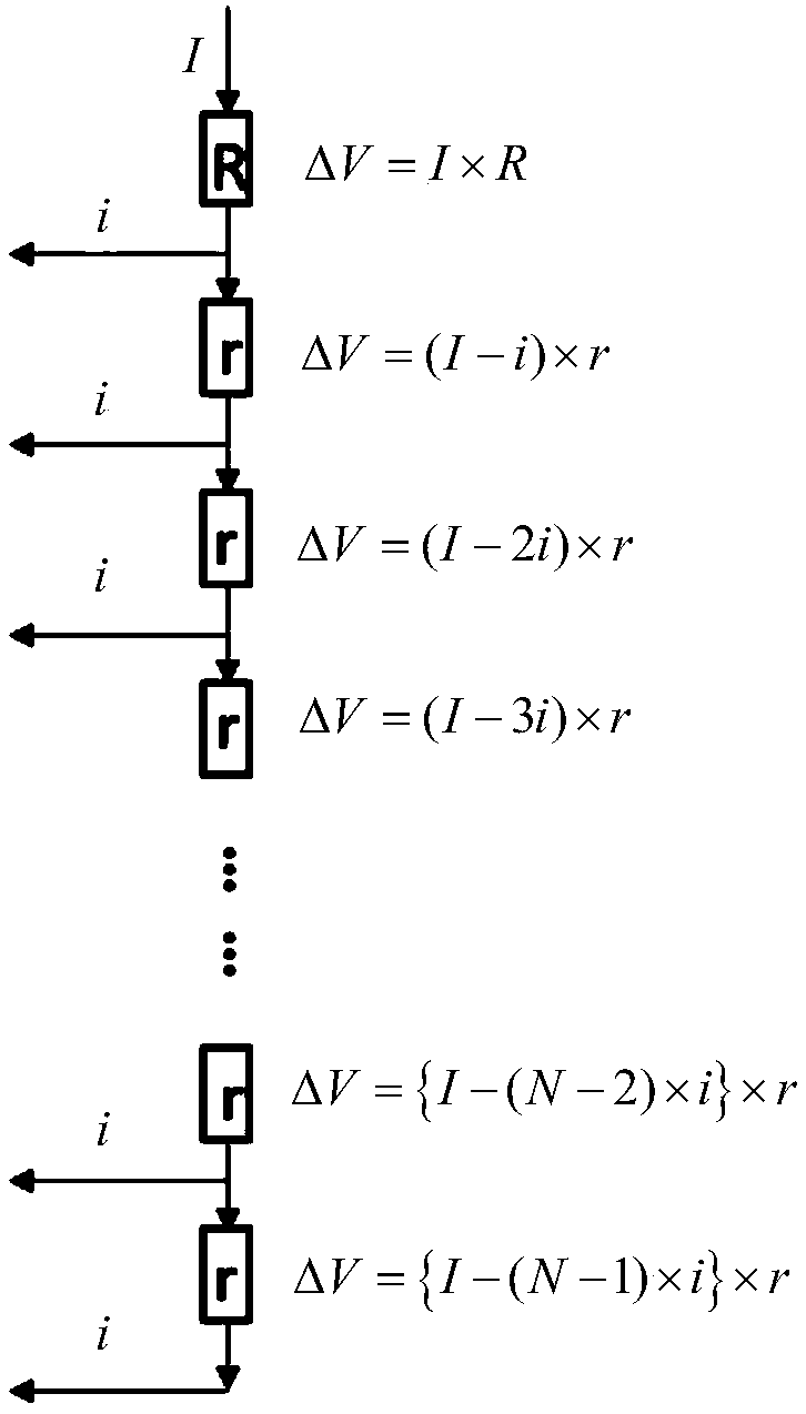
[0030] see figure 1 , the voltage drop compensation method provided by the embodiment of the pr...


PUM


Abstract

The embodiment of the invention discloses a voltage drop compensation method, a device thereof and a display device, which relate to the technical field of display and aim at compensating IR Drop of the display device to enhance the display effects of the display device. The voltage drop compensation method comprises steps: the impedance distribution of each pixel row of a display panel at the maximum display brightness is acquired, and a voltage drop model is built according to the impedance distribution of each pixel row; source-end input current of the display panel in the case of real-timedisplay is acquired, the source-end input current is used as an input value of the voltage drop model, and voltage drop corresponding to each pixel row is determined; and according to the voltage drop, a compensation gray scale of a corresponding pixel row is determined respectively, and according to each compensation gray scale, gray scale compensation is carried out on the corresponding row pixel respectively. The voltage drop compensation method, the device thereof and the display device provided in the embodiment of the invention are used for a large-size AMOLED display device.

Description

technical field [0001] The invention relates to the field of display technology, in particular to a voltage drop compensation method and its device, and a display device. Background technique [0002] With the development of science and technology, Active Matrix / Organic Light Emitting Diode (Active Matrix / Organic Light Emitting Diode) display device is recognized by the industry as the display device with the most development potential due to its advantages of lightness, thinness, bright color, and high contrast. [0003] At present, in order to meet users' pursuit of better visual effects, the panel size and resolution of AMOLED display devices are constantly increasing. However, for AMOLED display devices with large panel size and high resolution, when using the same power supply voltage (V DD ) when supplying power to each pixel unit in its display area, since the wires that transmit electrical signals corresponding to each pixel unit have different resistances, it is ea...

Claims


Application Information

Patent Timeline
Patent Type & Authority Applications(China)
IPC IPC(8): G09G3/3233
CPCG09G3/3233G09G2320/0233G09G2320/0223G09G2320/0271G09G2320/0276G09G2320/029G09G2360/16G09G3/3225G09G3/3291G09G2300/043
Inventor 谭文静赵辉
Owner BOE TECH GRP CO LTD
Why Eureka
Try Eureka