Isolation structure and production method thereof
A technology of isolation structure and manufacturing method, which is applied in semiconductor/solid-state device manufacturing, electrical components, circuits, etc., can solve the problems of poor hole filling ability and easy occurrence of particles in flowable dielectrics, so as to improve the performance of hole filling ability, Improve the effect of particles and avoid excessive stress
- Summary
- Abstract
- Description
- Claims
- Application Information
AI Technical Summary
Problems solved by technology
Method used
Image

Examples
Embodiment 1
[0082] The present invention provides a method for manufacturing an isolation structure, please refer to image 3 , is shown as a process flow chart of the method, comprising the steps:
[0083] Step S1 is first performed: providing a semiconductor substrate, the semiconductor substrate has a first surface and a second surface opposite to the first surface.
[0084] Specifically, the semiconductor substrate is a common semiconductor substrate. In this embodiment, the semiconductor substrate is an Si substrate as an example.
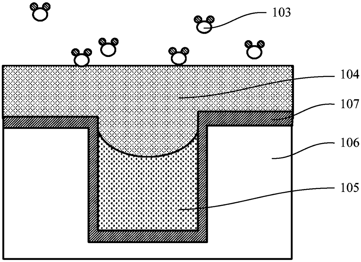
[0085] Step S2 is then performed: forming at least one trench in the substrate to define an active region, the trench forming an opening from the first surface and extending toward the second surface.
[0086] Specifically, first, a mask pattern of a groove is formed on the first surface of the semiconductor substrate by using photolithography techniques such as exposure and development, and then based on the mask pattern, a dry or wet etching technique ...
Embodiment 2
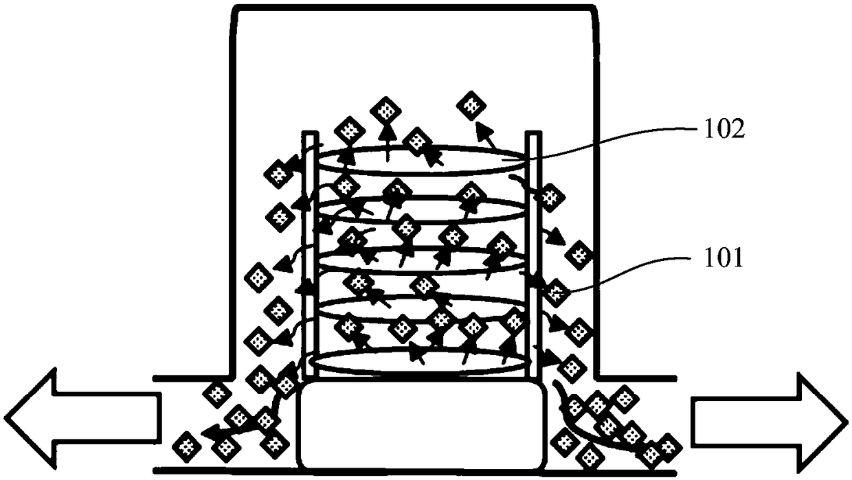
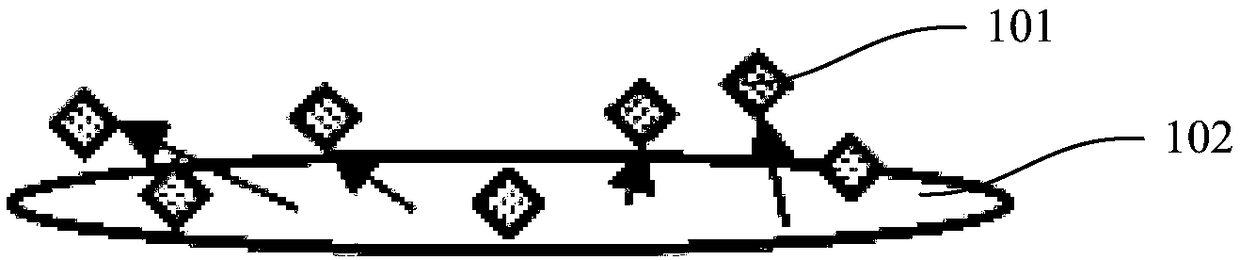
[0124] The present invention also provides an isolation structure, such as Figure 9 As shown, a schematic diagram of the isolation structure is shown, including:
[0125] A semiconductor substrate 201 has a first surface and a second surface opposite to the first surface, wherein at least one trench is formed in the semiconductor substrate 201 to define an active region, the trench forming an opening from the first surface and extending toward the second surface;
[0126] a liner layer 202 deposited on the sidewalls and bottom of the trench; and
[0127] A flowable dielectric is formed on the surface of the liner layer 202, the flowable dielectric fills the trench, and more than 90wt% of the flowable dielectric in the trench reacts as an oxide Isolator 203.
[0128] Specifically, the semiconductor substrate 201 includes but is not limited to a silicon substrate, the trench has an aspect ratio ranging from 14 to 18, and the material of the pad layer 202 includes at least on...
PUM
 Abstract
Description
Claims
Application Information
 - R&D Engineer
- R&D Manager
- IP Professional
- Industry Leading Data Capabilities
- Powerful AI technology
- Patent DNA Extraction
Browse by: Latest US Patents, China's latest patents, Technical Efficacy Thesaurus, Application Domain, Technology Topic.
© 2024 PatSnap. All rights reserved.Legal|Privacy policy|Modern Slavery Act Transparency Statement|Sitemap