A three-band switchable metamaterial absorber/reflector
A metamaterial and wave absorber technology, applied in antennas, electrical components, etc., to solve problems such as inability to apply electromagnetic waves
- Summary
- Abstract
- Description
- Claims
- Application Information
AI Technical Summary
Problems solved by technology
Method used
Image
Examples
Embodiment Construction
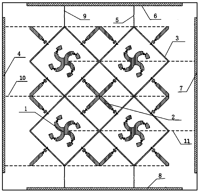
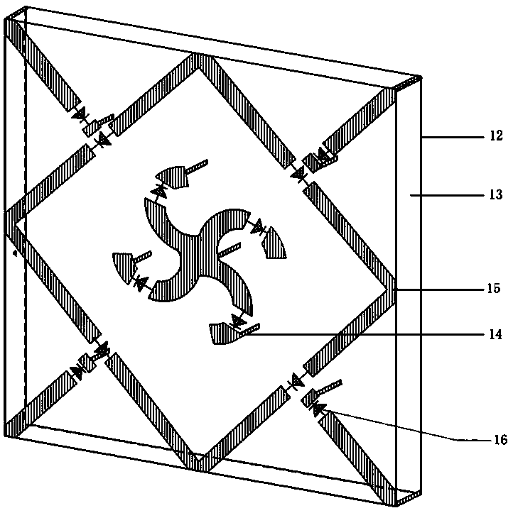
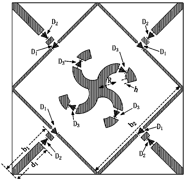
[0022] Using circuit board etching technology, open straight cross structure 2, open windmill structure 1, open square ring structure 3, open straight cross structure 2, The top of the open windmill structure 1 has a disconnection, and the middle part of the side of the open square ring structure 3 has a disconnection, such as Figure 1-Figure 3 As shown, a hole is punched at the top of the open straight cross structure 2 and the open windmill structure 1. The diameter of the hole is 0.6 mm, and the metal strip is penetrated to connect to the bottom metal plate 12. The size of the open straight cross structure 2 is b1=9.8 mm, d1=7.3mm, the line width is 1.4mm; the size of the open windmill structure 1 is R=3.5mm, h=0.4mm and the line width is 1.6mm; the size of the open square ring structure 3 is b2=21.21mm, the line width is 0.5mm; the unit crystal wrapping length is 30mm. The upper and lower bias lines (6, 8) control the silicon diode D in the split square ring structure 3 ...
PUM
| Property | Measurement | Unit |
|---|---|---|
| thickness | aaaaa | aaaaa |
| length | aaaaa | aaaaa |
Abstract
Description
Claims
Application Information


