Level conversion circuit

A technology for converting circuits and levels, applied in logic circuits, logic circuit connections/interface layouts, electrical components, etc., can solve problems such as low performance, achieve high-speed transmission performance, and improve the highest speed transmission capability

Pending Publication Date: 2018-12-18
SHANGHAI AWINIC TECH CO LTD
View PDF23 Cites 4 Cited by
  • Summary
  • Abstract
  • Description
  • Claims
  • Application Information

AI Technical Summary

Problems solved by technology

[0006] In view of this, the present invention provides a level conversion circuit to solve the problem of low performance of the level conversion circuit in the prior art under the condition of high-speed transmission

Method used


Image

  • Level conversion circuit
  • Level conversion circuit
  • Level conversion circuit

Examples


Embodiment Construction

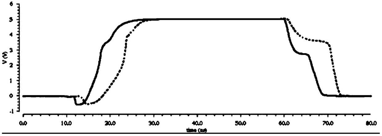
[0052] As mentioned in the background section, the level conversion circuit in the prior art has a limited maximum transmission speed, and the performance is lower when the transmission speed is higher.

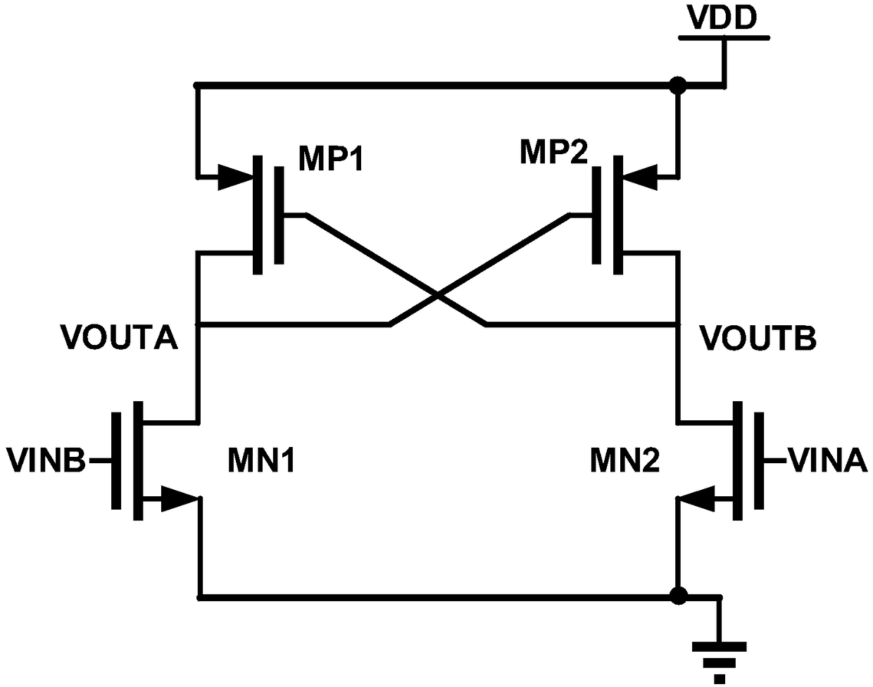
[0053] Such as figure 1 As shown, the input signals VINA and VINB of the level shift circuit are a pair of inverting signals in the low voltage domain, and the working positive power supply VDD is a high voltage power supply, respectively connected to the sources of the PMOS transistor MP1 and the PMOS transistor MP2. The sources of the NMOS transistor MN1 and the NMOS transistor MN2 are grounded. The drain of the PMOS transistor MP1, the gate of the PMOS transistor MP2 and the drain of the NMOS transistor MN1 are commonly connected to form an output terminal OUTA. The drain of the PMOS transistor MP2, the gate of the PMOS transistor MP1 and the drain of the NMOS transistor MN2 are commonly connected to form an output terminal OUTB. The output signals VOUTA and VOUTB are hi...


PUM


Abstract

A level conversion circuit is provided, a first impedance and a second impedance with constant resistance are added to that exist level conversion circuit to act as current limiting. By setting the positions of the first impedance and the second impedance, new capacitance is avoided to be introduced into the first impedance and the second impedance, thereby affecting the high-speed transmission performance of the level shifting circuit. In addition, the level conversion circuit provided by the invention can also have good high-speed transmission performance when the VDD voltage changes, especially when the VDD is low. And the highest speed transmission capability of the level shifting circuit is improved compared with the prior art level shifting circuit.

Description

technical field [0001] The invention relates to the technical field of electronic circuits, in particular to a level conversion circuit. Background technique [0002] In the design and development process of analog chips and System on Chip (SOC), due to the use of incompatible power supply voltages and other reasons, there are often problems with input / output logic inconsistencies within the system, so it is necessary to perform level convert. The level conversion circuit is used to convert the high-level signal and low-level signal (VINA, VINB) corresponding to the low-voltage domain into the high-level signal and low-level signal (VOUTA, VOUTB) corresponding to the high-voltage domain , or vice versa for an electronic circuit. [0003] That is to say, there may be multiple voltage domains in the analog chip and SOC system, and a level conversion circuit needs to be set up for control or clock signal transmission between different voltage domains. The low-voltage domain ...

Claims


Application Information

Patent Timeline
Patent Type & Authority Applications(China)
IPC IPC(8): H03K19/0185
CPCH03K19/018507
Inventor 何永强程剑涛杜黎明罗旭程张艳萍
Owner SHANGHAI AWINIC TECH CO LTD
Why Eureka
Try Eureka