Optical IC chip sampling machine with laser cutting function

A laser cutting and chip technology, applied in electrical components, semiconductor/solid-state device manufacturing, circuits, etc., can solve problems such as damage to eyes, secondary damage to chip strips, secondary damage to chips, etc., to achieve accurate inspection and avoid secondary damage. Secondary damage, the effect of avoiding artificial secondary damage

Active Publication Date: 2018-12-21
成都莱普科技股份有限公司
View PDF5 Cites 2 Cited by
  • Summary
  • Abstract
  • Description
  • Claims
  • Application Information

AI Technical Summary

Problems solved by technology

Chip strips cannot be touched by hand before packaging, otherwise it is easy to cause artificial secondary damage to the chip
In the traditional inspection of chip strips, the inspectors pull the chip strips by hand to observe under the microscope. For chip components with quality defects, it is necessary to manually hook the arcs, which causes the hands to touch the chip strips and damage the chips. Secondary damage to the strips; in addition, the human eye is prone to fatigue and damages the eyes when observing under a microscope for a long time

Method used


Image

  • Optical IC chip sampling machine with laser cutting function
  • Optical IC chip sampling machine with laser cutting function
  • Optical IC chip sampling machine with laser cutting function

Examples


Embodiment Construction

[0039] In order to make the object, technical solution and advantages of the present invention clearer, the present invention will be further described in detail below in conjunction with the accompanying drawings and embodiments. It should be understood that the specific embodiments described here are only used to explain the present invention, not to limit the present invention.

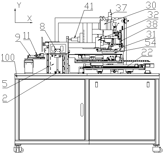
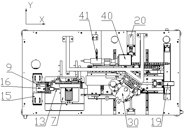
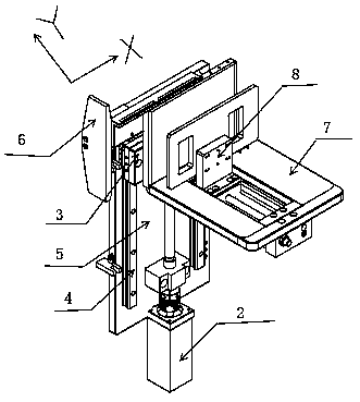
[0040] An IC chip optical sampling inspection machine with laser cutting function, comprising a frame body 100 and a material box mechanism installed on the frame body 100, a material pushing mechanism, a material retrieving mechanism, a transport mechanism, a microscope mechanism, a laser cutting mechanism, a microscope mechanism and The materials of the laser cutting mechanism are arranged side by side; the position of the material box mechanism can be adjusted up and down, X direction, and Y direction; the pushing mechanism can push the chip strips in the material box mechanism out of the materia...


PUM


Abstract

Provided in the invention is an optical IC chip sampling machine with the laser cutting function. The optical IC chip sampling machine comprises a rack body, a material box mechanism, a pushing mechanism, a reclaiming mechanism, a transport mechanism, a microscope mechanism, and a laser cutting mechanism. The location of the material box mechanism can be adjusted up and down or in an X direction or a Y direction. The pushing mechanism is able to push a chip stripe in the material box mechanism out of the material box mechanism. The reclaiming mechanism is able to clamping the chip stripe pushed out by the pushing mechanism on the transport mechanism. The transport mechanism transports the chip stripe to be under the microscope mechanism or transports the chip stripe to be under the laser cutting mechanism for cutting or marking. According to the invention, the whole chip stripe checking process including chip stripe selection, transport, observation, and processing is implemented without hand contact with the chip stripe, so that the manual secondary damage of the chip is avoided.

Description

technical field [0001] The invention relates to a chip sampling inspection machine, in particular to an IC chip optical sampling inspection machine with laser cutting function. Background technique [0002] Before packaging electronic chips, wire arcs and solder balls need to be inspected to avoid the impact of wire arcs and solder ball defects on chip performance and yield. Chip strips cannot be touched by hand before packaging, otherwise it is easy to cause artificial secondary damage to the chip. In the traditional inspection of chip strips, the inspectors pull the chip strips by hand to observe under the microscope. For chip components with quality defects, it is necessary to manually hook the arcs, which causes the hands to touch the chip strips and damage the chips. Secondary damage to the strips; in addition, the human eye is prone to fatigue and damages the eyes after observing under the microscope for a long time. Contents of the invention [0003] In view of th...

Claims


Application Information

Patent Timeline
Patent Type & Authority Applications(China)
IPC IPC(8): H01L21/67B07C5/02B07C5/342B07C5/36
CPCB07C5/02B07C5/3422B07C5/362H01L21/67271H01L21/67282H01L21/67288H01L21/67294
Inventor 何刘徐云潘冬徐万宇王德友陈永智唐道均蒲鹏周杰刘强魏启玉黄永忠
Owner 成都莱普科技股份有限公司
Why Eureka
Try Eureka