Circuit board, mobile terminal and circuit board wiring method

A technology of mobile terminals and circuit boards, which is applied in the direction of printed circuits, printed circuits connected with non-printed electrical components, electrical components, etc., can solve the problems of multi-line layout of components, limited PCB area, difficulties, etc., and achieve reduction The number of traces, solving the difficulty of trace layout, and reducing the effect of impedance

Active Publication Date: 2019-01-01
VIVO MOBILE COMM CO LTD
View PDF3 Cites 3 Cited by
  • Summary
  • Abstract
  • Description
  • Claims
  • Application Information

AI Technical Summary

Problems solved by technology

[0004] The embodiment of the present invention provides a PCB, a mobile terminal and a circuit board routing method to solve the problem of difficult routing layout caused by limited PCB area and many components

Method used


Image

  • Circuit board, mobile terminal and circuit board wiring method
  • Circuit board, mobile terminal and circuit board wiring method
  • Circuit board, mobile terminal and circuit board wiring method

Examples


Embodiment Construction

[0016] The following will clearly and completely describe the technical solutions in the embodiments of the present invention with reference to the accompanying drawings in the embodiments of the present invention. Obviously, the described embodiments are some of the embodiments of the present invention, but not all of them. Based on the embodiments of the present invention, all other embodiments obtained by persons of ordinary skill in the art without creative efforts fall within the protection scope of the present invention.

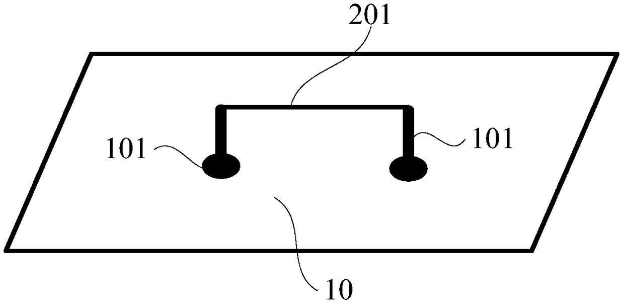
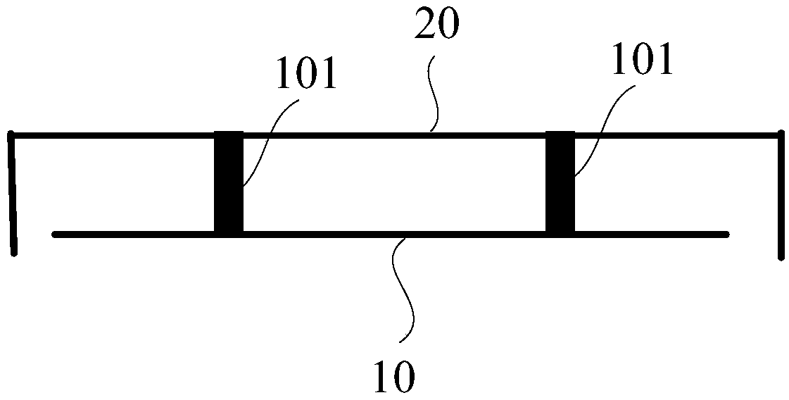
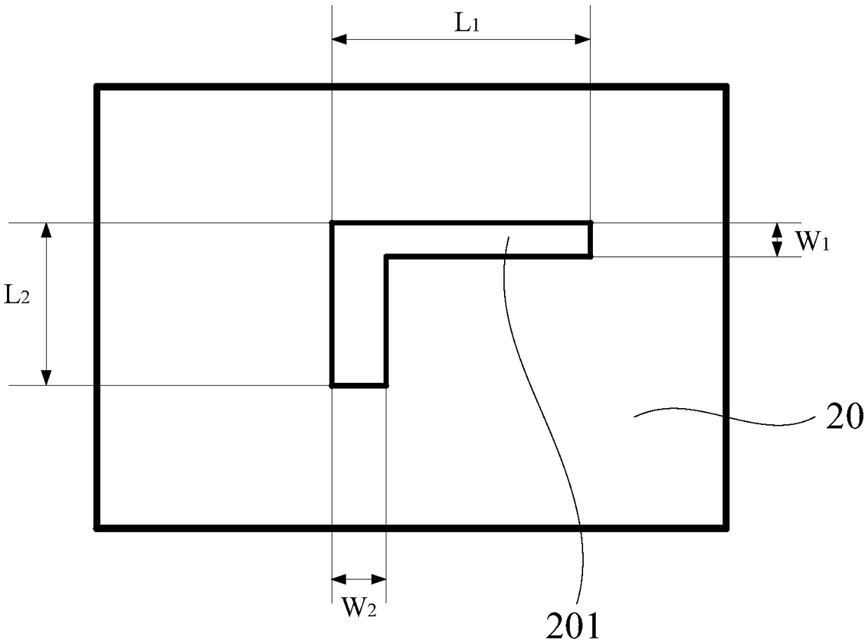
[0017] Such as figure 1 As shown, one embodiment of the present invention provides a PCB, including a PCB body 10, a plurality of components (not shown) are arranged on the PCB body 10, and wiring 201 between the plurality of components is arranged Outside the PCB body 10, the following will combine figure 1 The above PCB is introduced in detail.

[0018] The above-mentioned PCB body 10 can also be called a copper clad laminate, referred to as a copp...


PUM


Abstract

The embodiment of the invention discloses a printed circuit board (PCB), a mobile terminal and a PCB wiring method. The problem is solved that wiring layout is difficult caused by many components andparts due to the limited PCB area. The PCB comprises a PCB body, the PCB body is provided with components and parts, and wiring among the components and parts is arranged out of the PCB body. The problem is solved that wiring layout is difficult caused by many components and parts due to the limited PCB area, and the space utilization is increased. Besides, the wiring widths between the componentsand parts or the sections can be arranged to be enough large so as to reduce the wiring impedance and easily meet the impedance demands of PCB wiring.

Description

technical field [0001] The present invention relates to the field of terminals, in particular to a printed circuit board (Printed Circuit Board, PCB or circuit board for short), a mobile terminal and a wiring method for the circuit board. Background technique [0002] With the development of mobile terminal technology, the mobile terminal has more and more functions, and at the same time requires a larger and larger PCB area. On the contrary, due to the cost pressure of mobile terminals and the demand for battery life, the area that can be used on the PCB is getting smaller and smaller. It is difficult to meet the requirements of technical indicators such as impedance. [0003] The existing technology is to complete the wiring on the PCB plane. For power supplies with PDN (power distribution network, mainly DC impedance and AC impedance) requirements, the wiring width has been difficult to meet the requirements, which has become a bottleneck problem restricting the PCB. Ta...

Claims


Application Information

Patent Timeline
Patent Type & Authority Applications(China)
IPC IPC(8): H05K1/18
CPCH05K1/182H05K1/184
Inventor 覃荣敏
Owner VIVO MOBILE COMM CO LTD
Why Eureka
Try Eureka