Embedded type touch display panel

A touch display panel, embedded technology, applied in optics, instruments, electrical digital data processing and other directions, can solve the problem of limited number of signal transmission lines, large contact impedance, etc., to increase the coupling length, increase the signal-to-noise ratio, Effect of increasing side capacitance

Inactive Publication Date: 2018-07-13
WUHAN CHINA STAR OPTOELECTRONICS TECH CO LTD
View PDF9 Cites 2 Cited by
  • Summary
  • Abstract
  • Description
  • Claims
  • Application Information

AI Technical Summary

Problems solved by technology

[0005] like figure 1 As shown, it is an existing touch display panel, which includes: a plurality of driving electrodes 1 distributed in an array at intervals, and a plurality of sensing electrodes 2 arranged alternately and insulated from the plurality of driving electrodes 1 . Two adjacent sensing electrodes 2 are connected and two adjacent driving electrodes 1 are spaced apart. The two adjacent driving electrodes 1 are connected through a metal wire 3 insulated from the sensing electrodes 2 as a bridge, and mutual capacitance is used to realize contact In the prior art, the shape of the driving electrode 1 and the sensing electrode 2 are both diamond-shaped and the driving electrode 1 and the sensing electrode 2 are formed by cutting the common electrode layer, so that when the metal trace 3 overlaps with the driving electrode 1, the contact impedance is too high large, resulting in charge accumulation problems
With the development of touch display technology, terminal equipment puts forward higher requirements for touch LCD panels. The thickness of touch display panels needs to be made thinner and the display resolution is higher. Therefore, the signal transmission required There are more and more lines, and at the same time, in the case of continuous development of full screens, higher requirements are placed on the width of the border area of ​​the touch display panel. Although Chip-On-Film (COF ) scheme can narrow the border, but there are certain restrictions on the number of processes and signal transmission lines

Method used


Image

  • Embedded type touch display panel
  • Embedded type touch display panel
  • Embedded type touch display panel

Examples


Embodiment Construction

[0031] In order to further illustrate the technical means adopted by the present invention and its effects, the following describes in detail in conjunction with preferred embodiments of the present invention and accompanying drawings.

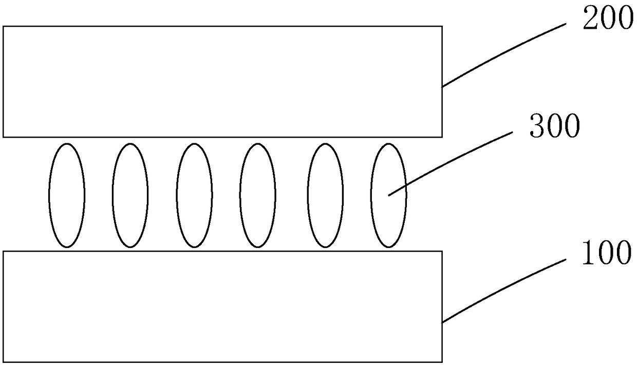
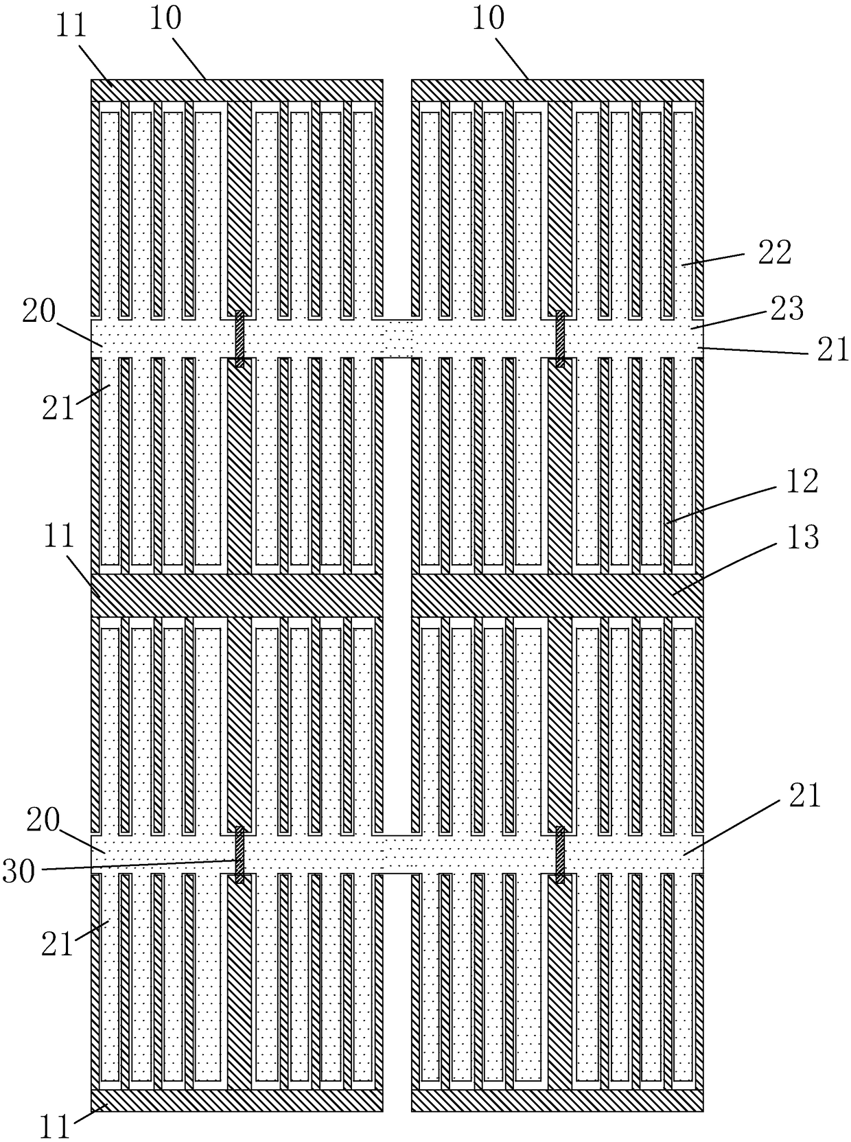
[0032] see Figure 2 to Figure 4 , the present invention provides an in-cell touch display panel, comprising: a TFT substrate 100 and a CF substrate 200 disposed opposite to each other, and a liquid crystal layer 300 disposed between the TFT substrate 100 and the CF substrate 200; the TFT substrate 100 includes: a first base substrate 101, and a first metal layer M1, a second metal layer M2, and a third metal layer M3 that are sequentially formed on the first base substrate 101 and insulated from each other;

[0033] The second metal layer M2 includes a plurality of bridging wires 30;

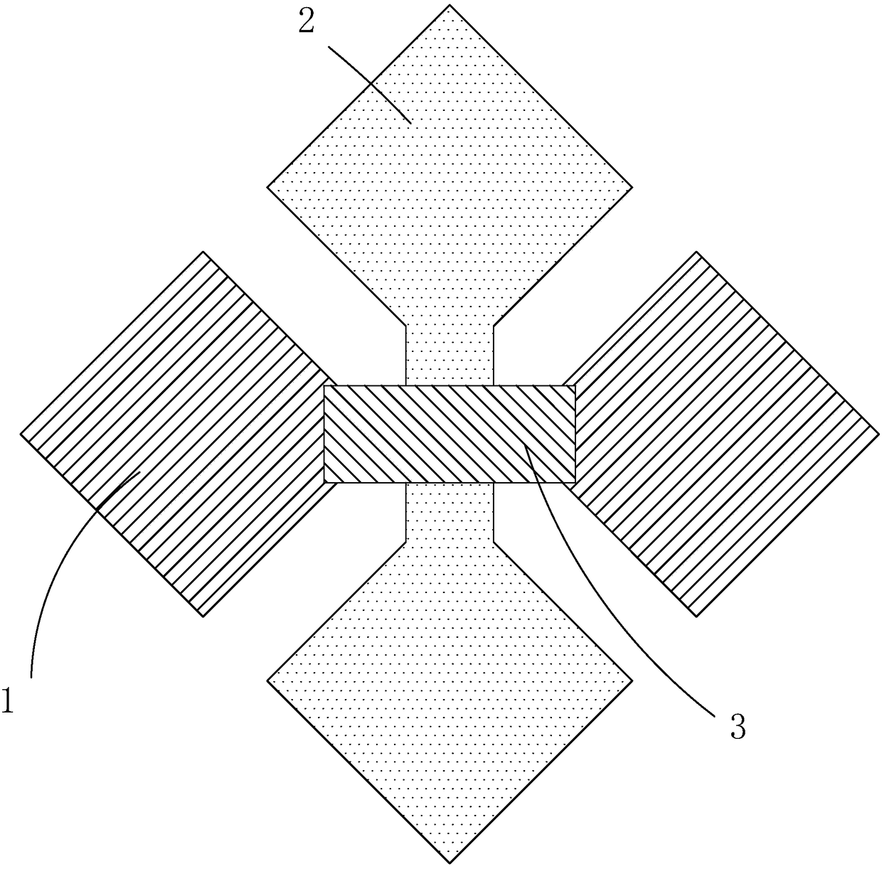
[0034] The third metal layer M3 includes a plurality of driving electrode strings 10 arranged in parallel in the longitudinal direction, and a plurality of se...


PUM


Abstract

The invention provides an embedded type touch display panel. A third metal layer is added to a TFT substrate, the third metal layer is adopted as a driving electrode and an induction electrode, the induction electrode comprises a plurality of parallel first vertical parts and a plurality of first horizontal parts perpendicularly connected with the first vertical parts, and the driving electrode comprises a plurality of parallel second vertical parts and a plurality of second horizontal parts perpendicularly connected with the second vertical parts; the multiple second vertical parts and the multiple first vertical parts are staggered and distributed in the longitudinal direction; every two adjacent second vertical parts of the driving electrode are connected through bridging wiring in a second metal layer, the mutual capacitance touch function is achieved, the coupling length between the driving electrode and the induction electrode can be increased to increase lateral capacitance between the driving electrode and the induction electrode, the integration level of a display panel is increased, charge gathering caused at the bridging position of the driving electrode is lowered whilethe number of touch signal wires is decreased, the touch performance and the user experience are improved, and the signal to noise ratio is increased.

Description

technical field [0001] The present invention relates to the field of display technology, in particular to an embedded touch display panel. Background technique [0002] With the development of display technology, liquid crystal displays (Liquid Crystal Display, LCD) and other flat display devices are widely used in mobile phones, televisions, personal Various consumer electronic products such as digital assistants, digital cameras, notebook computers, and desktop computers have become the mainstream of display devices. [0003] Most of the liquid crystal displays currently on the market are backlight liquid crystal displays, which include a liquid crystal display panel and a backlight module. The working principle of the liquid crystal display panel is to pour liquid crystal molecules between the thin film transistor array substrate (ThinFilm Transistor Array Substrate, TFT Array Substrate) and the color filter (ColorFilter, CF) substrate, and apply a driving voltage on the...

Claims


Application Information

Patent Timeline
Patent Type & Authority Applications(China)
IPC IPC(8): G02F1/1333G02F1/1343G06F3/041G06F3/044
CPCG02F1/13338G02F1/134309G06F3/0412G06F3/044
Inventor 石腾腾李东霖胡巧
Owner WUHAN CHINA STAR OPTOELECTRONICS TECH CO LTD
Why Eureka
Try Eureka