Electrolytic nickel (ALLOY) plating solution

A plating solution and electrolytic nickel technology, applied in circuits, electrical components, printed circuits, etc., can solve problems such as insufficient filling of tiny holes, tiny recesses, insufficient filling of electrolytic nickel plating solution, and cracks in precipitates.

Active Publication Date: 2019-01-04
JAPAN PURE CHEM
View PDF5 Cites 0 Cited by
  • Summary
  • Abstract
  • Description
  • Claims
  • Application Information

AI Technical Summary

Problems solved by technology

[0011] However, according to the additional tests conducted by the present inventors (example described later), it was found that the filling property of the electrolytic nickel plating solution described in Non-Patent Document 2 was not sufficient to suppress the generation of voids, and in addition, deposits would Cracks are generated, which is bad as a structure
[0012] The miniaturization of electronic circuits is progressing vigorously. In related known technologies, the filling performance of microscopic holes and microscopic recesses is not sufficient, and it is desired to develop a nickel filling method that does not cause defects such as holes or cracks.

Method used


Image

  • Electrolytic nickel (ALLOY) plating solution
  • Electrolytic nickel (ALLOY) plating solution
  • Electrolytic nickel (ALLOY) plating solution

Examples


Embodiment 1 to 4、 comparative example 1 to 3

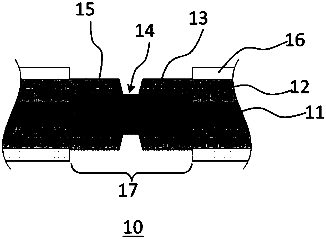
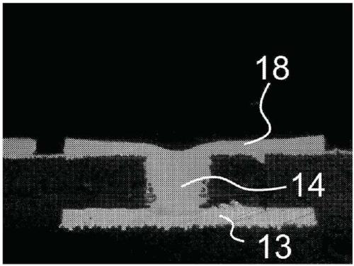
[0101] A 12 mm square evaluation printed circuit board (manufactured by Nippon Circuit Co., Ltd.) having a laser hole with an aspect ratio of 0.88 (φ45 μm×40 μmD) was used as a model of the minute concave portion.

[0102] A sectional view of the periphery 10 of the plated portion is shown in figure 1 . Copper foil 13 with a thickness of 12 μm is attached to the through-hole forming part of the base material 11 made of BT (Bismaleimide-triazine) with a thickness of 0.4 mm, and a prepreg with a thickness of 60 μm is laminated thereon. After prepreg type build-up resin (build-up resin) 12, a blind via hole (blind via hole) with a diameter of 45 μm and a depth of 40 μm (hereinafter also referred to as “via hole” and “ In the case of a "via" 14, a seed layer 15 of about 1 μm is formed on the outer surface of the substrate (the surface of the build-up resin 12) and the inner wall of the through hole 14 by electroless copper plating.

[0103] Furthermore, it is formed by dry film ...


PUM


Abstract

The present invention addresses the problem of providing: an electrolytic nickel (alloy) plating solution which is able to fill micro holes or micro recesses 14 within an electronic circuit componentwith nickel or nickel alloy 18 without the generation of defects such as voids and seams; a nickel or nickel alloy plating / filling method which uses this electrolytic nickel (alloy) plating solution;and a method for producing a three-dimensional microstructure. The above-described problem has been solved by filling the micro holes or micro recesses 14 with use of an electrolytic nickel (alloy) plating solution which contains a specific N-substituted carbonyl pyridinium compound.

Description

technical field [0001] The present invention relates to an electrolytic nickel plating solution or an electrolytic nickel alloy plating solution (hereinafter, these are also collectively referred to as "electrolytic nickel (alloy) plating solution"). Electrolytic nickel (alloy) plating solution for plating and filling tiny holes or tiny recesses in circuit components. [0002] In addition, the present invention also relates to a method of plating and filling microscopic holes or microscopic recesses using the electrolytic nickel (alloy) plating solution, and a method of manufacturing a microscopic three-dimensional structure. Background technique [0003] Electronic circuit components represented by semiconductors or printed circuit boards have micro holes or micro recesses such as vias, through holes, and trenches for forming wiring. In the past, when laminating multiple circuit boards to manufacture multi-layer printed circuit boards, the staggered via structure is the ma...

Claims


Application Information

Patent Timeline
Patent Type & Authority Applications(China)
IPC IPC(8): C25D3/12
CPCC25D3/12C25D3/18C25D7/123H05K3/241
Inventor 柴田和也大平原祐树
Owner JAPAN PURE CHEM
Why Eureka
Try Eureka