FPGA prototype verification system

A prototype verification and port technology, applied in CAD circuit design, special data processing applications, instruments, etc., can solve problems such as insufficient support for large-scale data exchange, small number of interconnection interfaces, etc., to facilitate module or full-chip prototype verification experiments , Solve the effect of less interconnection interface

Pending Publication Date: 2019-01-11
天津市滨海新区信息技术创新中心 +1
View PDF4 Cites 10 Cited by
  • Summary
  • Abstract
  • Description
  • Claims
  • Application Information

AI Technical Summary

Problems solved by technology

[0006] However, in the current FPGA verification system, the number of interconnection interfaces between every two FPGA chips is relatively small, which is not enough to support large-scale data exchange

Method used


Image

  • FPGA prototype verification system
  • FPGA prototype verification system
  • FPGA prototype verification system

Examples


Embodiment Construction

[0033] In order to make the purpose, technical solutions and advantages of the embodiments of the present invention clearer, the technical solutions of the present invention will be clearly and completely described below in conjunction with the accompanying drawings. Obviously, the described embodiments are part of the embodiments of the present invention, not all of them. the embodiment. Based on the embodiments of the present invention, all other embodiments obtained by persons of ordinary skill in the art without making creative efforts belong to the protection scope of the present invention.

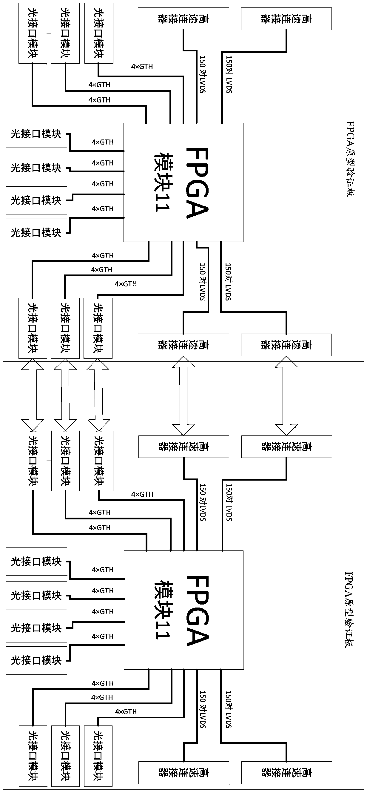
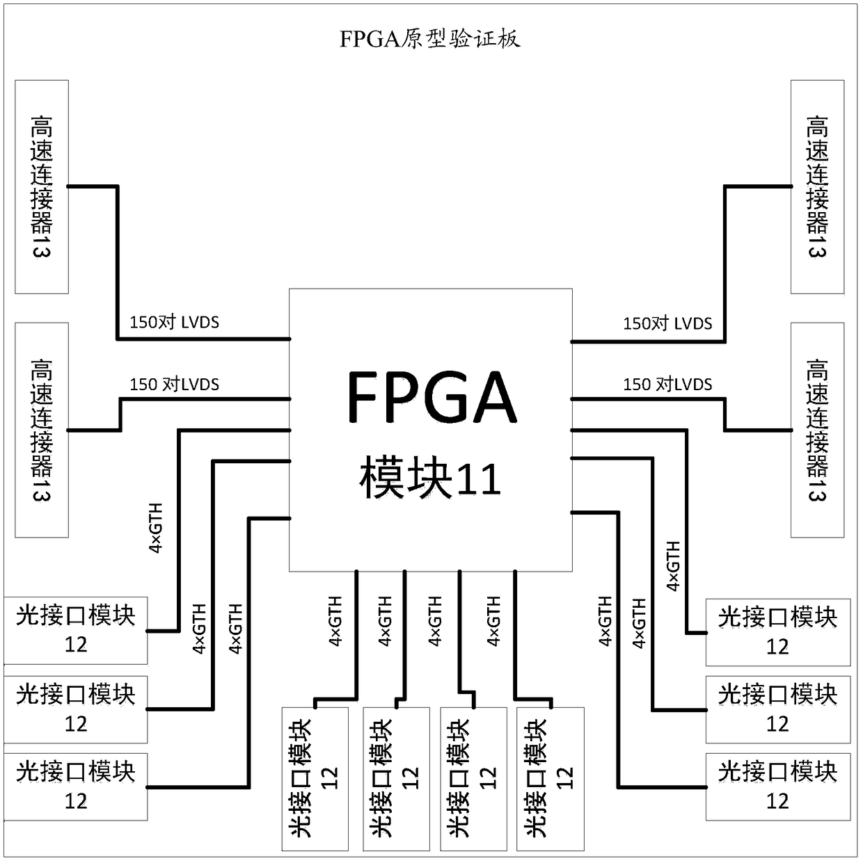
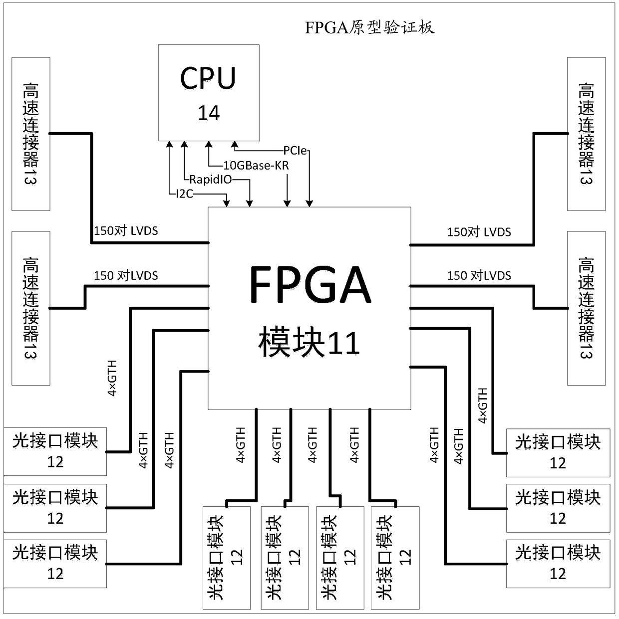
[0034] In the current FPGA verification system, the number of interconnection interfaces between each two FPGA chips is relatively small, which is not enough to support large-scale data exchange. For example, the VU440 cascade verification board needs to meet the basic requirements of resources and interfaces in a single exchange verification scenario. At the same time, due to the la...


PUM


Abstract

The invention provides an FPGA prototype verification system. The FPGA prototype verification system comprises at least two cascaded FPGA prototype verification boards. The I/O port of the high-speedconnector of the FPGA prototype verification board of the previous stage is connected with the I/O port of the high-speed connector of the FPGA prototype verification board of the next stage. The I/Oport of the optical interface module of the preceding FPGA prototype verification board is connected with the I/O port of the optical interface module of the subsequent FPGA prototype verification board. Through the high-speed connector and the optical interface module, the board-level cascading can be flexibly carried out, thereby facilitating some large-scale module or whole-chip prototype verification experiments, and the technical effect that the available interconnection interface is greatly improved to solve the shortcoming of the existing scheme that the interconnection interface is few.

Description

technical field [0001] The invention relates to the technical field of FPGA prototype verification, in particular to an FPGA prototype verification system. Background technique [0002] FPGA prototyping is a well-established technique for verifying the functionality of application-specific integrated circuits (ASICs), application-specific standard products (ASSPs) and systems-on-chip (SoCs) by porting RTL to field-programmable gate arrays (FPGAs) and performance. [0003] It is used even more widely today due to the increasing complexity of hardware and the increasing amount of associated software that needs to be verified. [0004] Since this software typically accounts for more than half of the design effort, the FPGA implementation of SoC RTL can also be used as the basis for software development, hardware / software co-verification, and software verification—all before final silicon is available. [0005] All of these factors help reduce design cost and time to market, r...

Claims


Application Information

Patent Timeline
Patent Type & Authority Applications(China)
IPC IPC(8): G06F17/50
CPCG06F30/398G06F30/34
Inventor 赵玉林吕平刘勤让沈剑良张霞汪欣张波王盼朱珂王锐张进李杨毛英杰李庆龙董春雷
Owner 天津市滨海新区信息技术创新中心
Why Eureka
Try Eureka