Pixel circuit, pixel drive method and display device

A technology for pixel circuits and driving units, applied in circuits, electrical components, static indicators, etc., can solve problems such as time extension, inconsistent initial state, afterimage, etc., and achieve the effect of improving afterimage and reducing hysteresis effect.

Inactive Publication Date: 2019-01-22
BOE TECH GRP CO LTD +1
View PDF6 Cites 20 Cited by
  • Summary
  • Abstract
  • Description
  • Claims
  • Application Information

AI Technical Summary

Problems solved by technology

[0003] After the OLED display panel displays a black and white checkerboard image for a period of time, the grayscale of the display image of the OLED display panel is controlled to be uniformly switched to grayscale 48, because the initial states of the existing drive transistors are inconsistent (in the pixel circuit displaying a white image The initial potential of the source of the driving transistor is V_L255, and the initial potential of the source of the driving transistor in the pixel circuit displaying a black screen is V_L0, where V_L255 is the data voltage corresponding to gray scale 255, and V_L0 is the data corresponding to gray scale 0 Voltage), due to the response speed of the driving transistor, it will lead to a prolonged time to reach the same brightness (such as the brightness corresponding to gray scale 48), that is, when the same data voltage is written, the corresponding current is inconsistent, resulting in inconsistent display brightness. afterimage

Method used


Image

  • Pixel circuit, pixel drive method and display device
  • Pixel circuit, pixel drive method and display device
  • Pixel circuit, pixel drive method and display device

Examples


Embodiment Construction

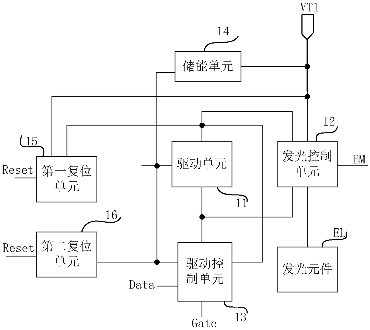
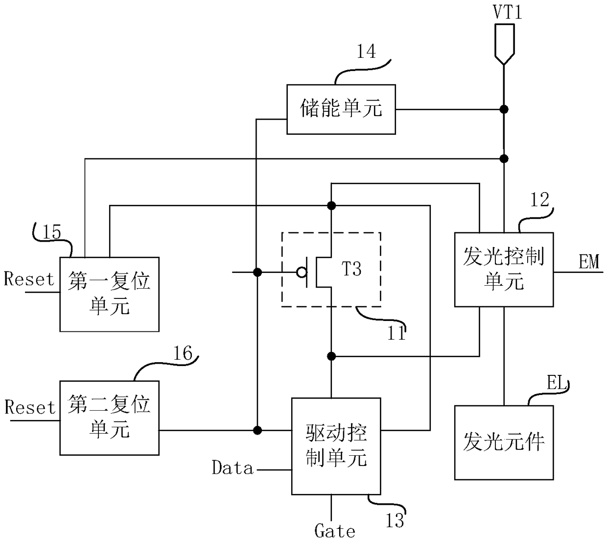
[0059] The following will clearly and completely describe the technical solutions in the embodiments of the present invention with reference to the accompanying drawings in the embodiments of the present invention. Obviously, the described embodiments are only some, not all, embodiments of the present invention. Based on the embodiments of the present invention, all other embodiments obtained by persons of ordinary skill in the art without making creative efforts belong to the protection scope of the present invention.

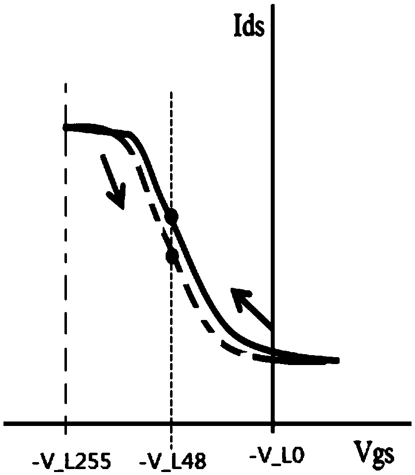
[0060] The transistors used in all the embodiments of the present invention can be thin film transistors or field effect transistors or other devices with the same characteristics. In the embodiment of the present invention, in order to distinguish the two poles of the transistor except the gate, one pole is called the first pole, and the other pole is called the second pole. In actual operation, the first electrode may be a drain, and the second electrode may...


PUM


Abstract

The invention provides a pixel circuit, a pixel drive method and a display device. The pixel circuit comprises a light-emitting element, a drive unit, a light emitting control unit, a drive control unit, an energy storage unit, a first reset unit and a second reset unit, wherein the first reset unit is used for controlling first voltage output by a first voltage line to be written into a first endof the drive unit under the control of a rest control line; the second reset unit is used for controlling initial voltage output by an initial voltage line to be written into a control end of the drive unit under the control of the rest control line; and the drive unit is used for driving the light-emitting element to emit light under the control of the control end of the drive unit. With the pixel circuit, the pixel drive method and the display device, the problem of residual image display caused by the retardation effect of a drive transistor of the drive unknit in the prior art is solved.

Description

technical field [0001] The present invention relates to the field of display technology, in particular to a pixel circuit, a pixel driving method and a display device. Background technique [0002] Afterimages have always been a difficult problem in OLED display devices, and the cause of afterimages is the hysteresis effect of the driving transistor. The technological solutions adopted in the prior art have little effect on improving the afterimage problem. Since only the gate potential of the driving transistor is reset during the reset phase in the prior art, and the potential of the source of the driving transistor still maintains the gray-scale voltage of the adjacent previous frame, an afterimage phenomenon will occur, as follows: [0003] After the OLED display panel displays a black and white checkerboard image for a period of time, the grayscale of the display image of the OLED display panel is controlled to be uniformly switched to grayscale 48, because the initial...

Claims


Application Information

Patent Timeline
Patent Type & Authority Applications(China)
IPC IPC(8): G09G3/3291G09G3/3258
CPCG09G3/3258G09G3/3291G09G2320/0257G09G2300/0426G09G2300/0819G09G2310/0216H10K59/131
Inventor 黄应龙杨炳伟高文宝
Owner BOE TECH GRP CO LTD
Why Eureka
Try Eureka