Finite Element Simulation Method for Determining the Complete Rule of Solder Joint Damage Accumulation in Irregular Thermal Profile

A simulation method and finite element technology, applied in design optimization/simulation, special data processing applications, instruments, etc., can solve the problems of high cost and long experiment period, and achieve the effect of accurate results, long compensation period and easy to obtain.

Active Publication Date: 2019-02-26
BEIHANG UNIV
View PDF3 Cites 7 Cited by
  • Summary
  • Abstract
  • Description
  • Claims
  • Application Information

AI Technical Summary

Benefits of technology

This patented technology uses simulations that predict how cracks will occur when subjected to heat or mechanical stress during use without requiring expensive equipment such as lasers. It also considers factors like material size and shape affecting this process, resulting in better accuracy compared to previous models. Overall, it provides technical benefits over existing techniques but at lower costs due to its simplicity and ease-of-use features.

Problems solved by technology

This patented technical solution describes how to improve the performance of electronic devices by reducing their risk of experiencing failures due to heat cycles over time caused by repeated use or exposure during normal operation. Current methods involve testing various factors such as mechanical properties (stress) and environmental effects like temperatures outside specific ranges. These tests require extensive experimentation and expensive laboratory facilities, making them difficult to perform frequently enough to identify any issues related to improving durable electronics designs without requiring excessive effort.

Method used


Image

  • Finite Element Simulation Method for Determining the Complete Rule of Solder Joint Damage Accumulation in Irregular Thermal Profile
  • Finite Element Simulation Method for Determining the Complete Rule of Solder Joint Damage Accumulation in Irregular Thermal Profile
  • Finite Element Simulation Method for Determining the Complete Rule of Solder Joint Damage Accumulation in Irregular Thermal Profile

Examples


specific Embodiment

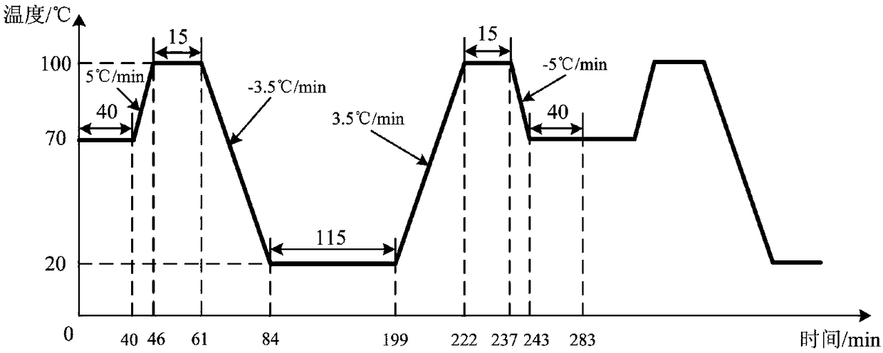
[0121] Taking an aircraft inertial navigation system that performs missions in summer as an example, the finite element simulation method of the damage accumulation law under the irregular temperature cycle profile of the solder joints of BGA packaged devices in its electronic equipment is illustrated. The specific steps of the method are as follows:

[0122] S1. Pre-processing of finite element simulation:

[0123] S11. Determine the components and package form of the finite element three-dimensional structural model, and determine the mesh division method of the model. The finite element model of the chip is packaged in the form of 16mm×16mm BGA, and the chip size is 25mm×25mm. The finite element three-dimensional structure model includes five parts: solder joints, chips, substrates, plastic packaging layers, and PCB layers. The chip information is input into ANSYS software, and Sweeping technology is used to generate octahedral units for solder joints, and hexahedral units...


PUM


Abstract

The invention provides a finite element simulation method for determining a complete rule of solder joint damage accumulation under an irregular temperature-following profile. The method comprises thefollowing steps: S1, a finite element simulation pretreatment; S2, finite element simulation of solder joints under different temperature loads, S3, finite element simulation post-processing, S4, determination of the nonlinear damage accumulation expression of solder joints under irregular temperature profile. The nonlinear damage accumulation rule determined by the simulation method is based ona fatigue crack damage model of a solder joint, Compared with the traditional method based on statistics, this method is more practical and takes into account the influence of stacking sequence of different temperature profiles. The result is more accurate, and the error can be controlled within 8%, which greatly reduces the error range.

Description


Claims


Application Information

Patent Timeline
Owner BEIHANG UNIV
Why Eureka
Try Eureka