Film slitting device and film slitting method

A film device and cutter technology, applied in metal processing, electrical components, semiconductor/solid-state device manufacturing, etc., can solve the problem of wafer groove film covering and other issues

Inactive Publication Date: 2019-02-26
ZHISHENG SCI & TECH GUANGZHOU
View PDF8 Cites 4 Cited by
  • Summary
  • Abstract
  • Description
  • Claims
  • Application Information

AI Technical Summary

Problems solved by technology

[0005] In view of the above problems, the present invention discloses a film cutting device and a film cutting method, which help to solve the problem that the wafer groove will be covered by an incompletely cut film

Method used


Image

  • Film slitting device and film slitting method
  • Film slitting device and film slitting method
  • Film slitting device and film slitting method

Examples


Embodiment Construction

[0059] The detailed features and advantages of the present invention are described in detail below in the implementation manner, and its content is enough to make any person skilled in the art understand the technical content of the present invention and implement it accordingly, and according to the content disclosed in this specification, the scope of protection of the claims and With the accompanying drawings, any person skilled in the art can easily understand the related objects and advantages of the present invention. The following examples further illustrate the concept of the present invention in detail, but do not limit the scope of the present invention in any way.

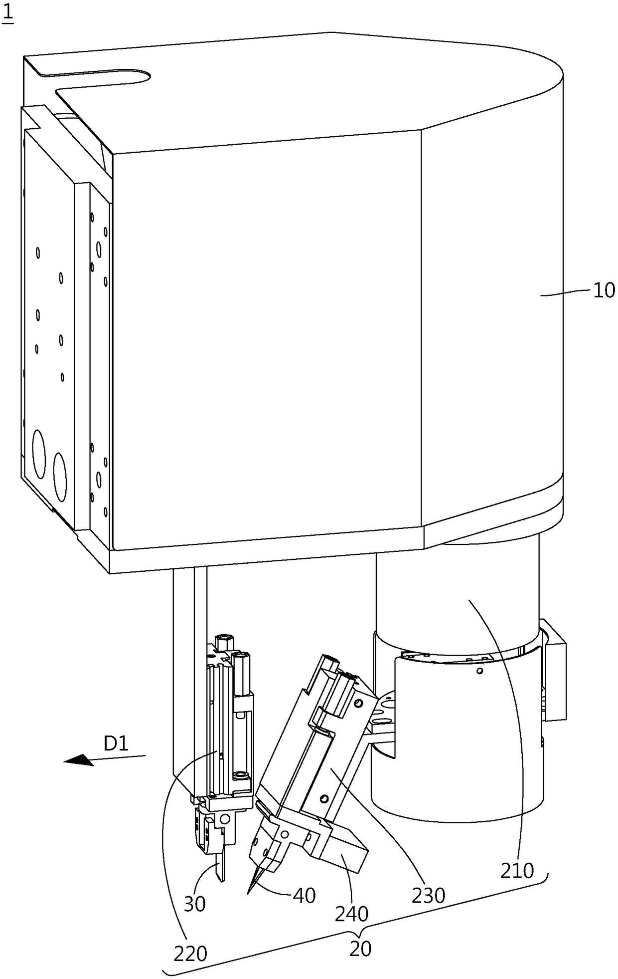
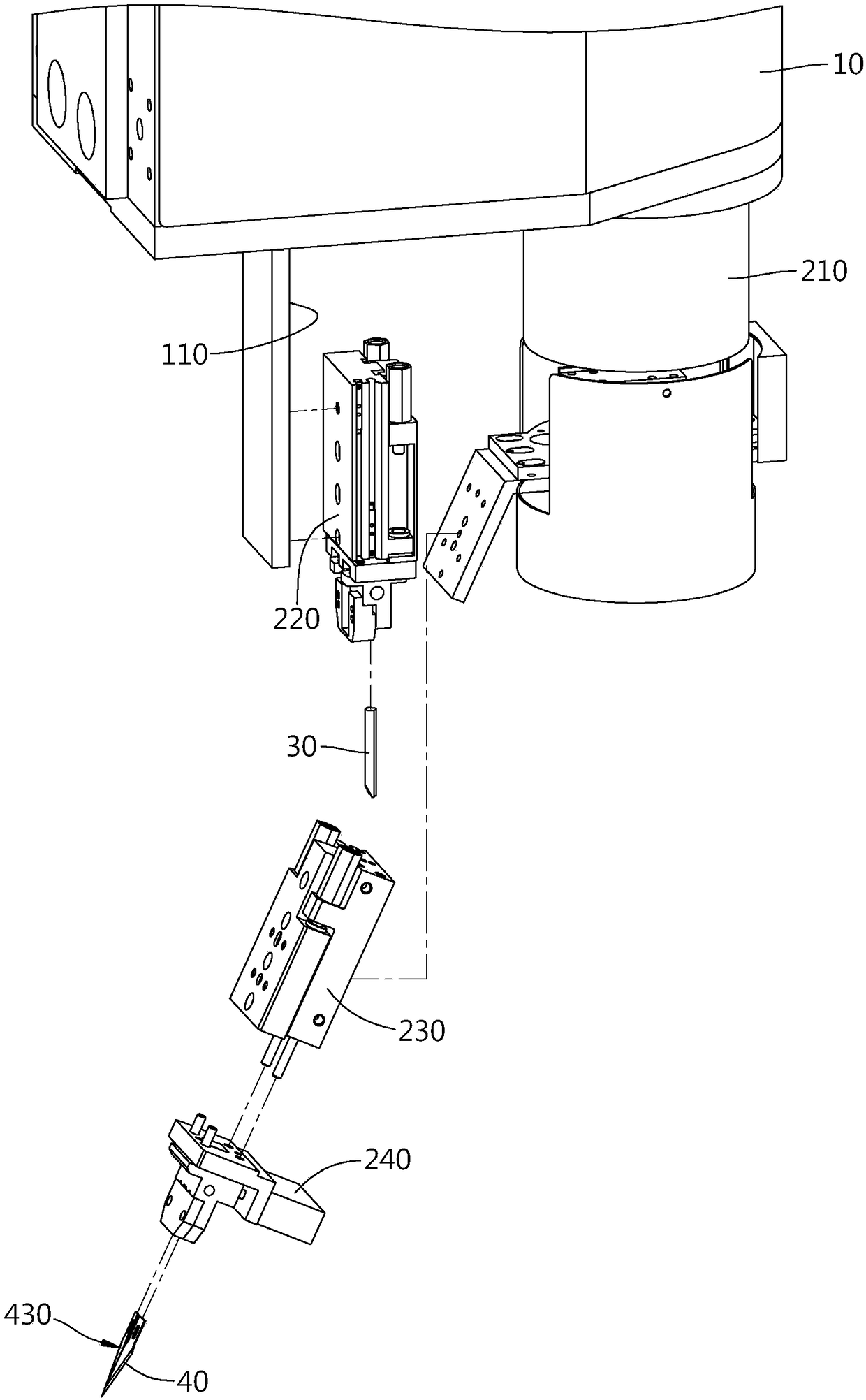
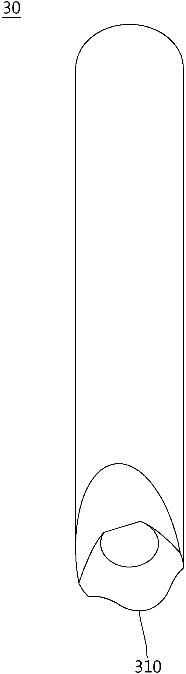
[0060] Please also refer to Figure 1 to Figure 2 . figure 1 It is a three-dimensional schematic diagram of a film cutting device according to an embodiment of the present invention. figure 2 for figure 1 An exploded schematic of the film-slitting device. In this embodiment, the film cutting device ...


PUM


Abstract

The present invention discloses a film slitting device configured to cut a thin film suitable for attaching to a wafer, wherein the wafer has an outer edge and a groove located at the outer edge. Thefilm slitting device comprises a bearing seat, a motion module, a groove cutter and an outer edge cutter. The motion module is arranged at the bearing seat. The groove current is arranged at the motion module to allow the motion module to drive the groove cutter to move relative to the bearing seat to be close to or far away from the thin film. The groove cutter can cut the thin film to form a broken hole at the thin film. The outer edge cutter is arranged at the motion module to allow the motion module to drive the outer edge cutter to move relative to the groove cutter to be close to or faraway from the thin film. The motion module can drive the outer edge cutter to rotate relative to the bearing seat to cut the thin film. The present invention further discloses a film slitting method.

Description

technical field [0001] The present invention relates to a film cutting device and a film cutting method thereof, in particular to a film cutting device and a film cutting method for cutting a film attached to a wafer surface with a knife. Background technique [0002] In the manufacturing process of semiconductor integrated circuits and various micro-electromechanical devices, one of the steps is to attach a thin film on the surface or back of the wafer (Wafer) for subsequent related wafer manufacturing processes. Films for attaching to wafers include but are not limited to dicing blue film, dicing white film, thinned protective film, UV film, and DAF (DieAttach Film) conductive film. Generally speaking, when attaching the film, the width of the film will be larger than the size of the wafer, so that the wafer can be fully covered. However, after attaching the film on the wafer, if the film is not well attached to the surface of the wafer or the edge of the film is too larg...

Claims


Application Information

Patent Timeline
Patent Type & Authority Applications(China)
IPC IPC(8): H01L21/67B26D1/04
CPCB26D1/045H01L21/67092
Inventor 曾永村陈明宗杨佳裕
Owner ZHISHENG SCI & TECH GUANGZHOU
Why Eureka
Try Eureka