
Semiconductor IC component and part size measurement method and device, and terminal device

A measuring method and technology of measuring device, applied in measuring device, using optical device, instrument, etc., can solve the problem of inaccurate size of measuring components

Active Publication Date: 2019-03-01
东莞市北井光控科技有限公司
View PDF10 Cites 9 Cited by
  • Summary
  • Abstract
  • Description
  • Claims
  • Application Information

AI Technical Summary

Problems solved by technology

[0004] In view of this, the embodiment of the present application provides a semiconductor IC component size measurement method, device and terminal equipment to solve the problem of inaccurate measurement of component size in the prior art

Method used


Image

  • Semiconductor IC component and part size measurement method and device, and terminal device
  • Semiconductor IC component and part size measurement method and device, and terminal device
  • Semiconductor IC component and part size measurement method and device, and terminal device

Examples


Embodiment Construction

[0096] In the following description, specific details such as specific system structures and technologies are presented for the purpose of illustration rather than limitation, so as to thoroughly understand the embodiments of the present application. It will be apparent, however, to one skilled in the art that the present application may be practiced in other embodiments without these specific details. In other instances, detailed descriptions of well-known systems, devices, circuits, and methods are omitted so as not to obscure the description of the present application with unnecessary detail.

[0097] In order to illustrate the technical solutions described in this application, specific examples are used below to illustrate.

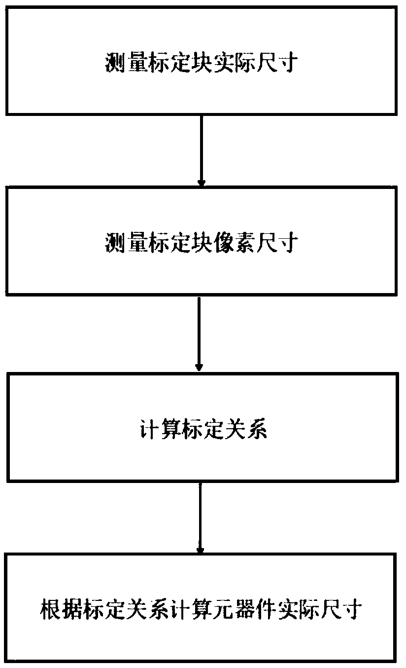
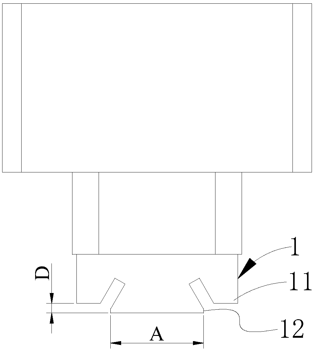
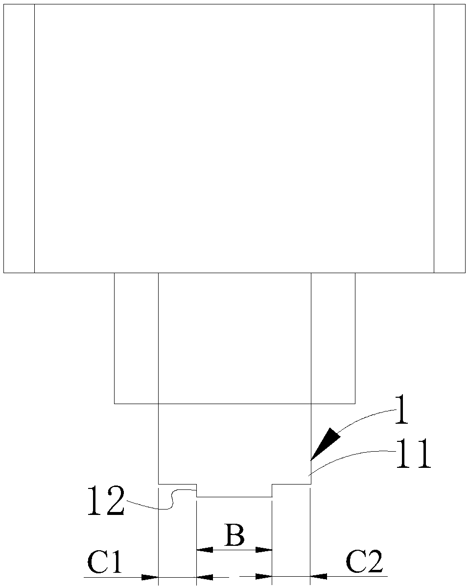
[0098] see Figure 1 to Figure 7 , which is a preferred embodiment provided by the present invention, and this embodiment relates to a method for measuring the size of semiconductor IC components, wherein, the semiconductor IC components in this embo...


PUM


Abstract

The present invention provides a semiconductor IC component and part size measurement method and device, and a terminal device. The semiconductor IC component and part size measurement method comprises the steps of: obtaining the actual size of a calibration block, and measuring the pixel size of the calibration block through a visual measurement module; according to the actual size of the calibration block and the pixel size of the calibration block, determining a conversion relation of the pixel size and the actual size; and obtaining the pixel sizes of the components and the parts, and combining the conversion relation to calculate and obtain the actual sizes of the components and the parts. Therefore, through the actual size of the calibration block and the pixel size of the calibration block, the conversion relation of the pixel size and the actual size is determined and the pixel sizes of the components and the parts and the conversion relation are combined to simply and accurately calculate and obtain the actual sizes of the components and the parts.

Description

technical field [0001] The application belongs to the field of machine vision recognition, and in particular relates to a method, device and terminal equipment for measuring the size of semiconductor IC components. Background technique [0002] In the production and processing process of components, in order to ensure the precision of components, it is usually necessary to test components, such as various semiconductor chips. At present, the more commonly used method is to inspect or measure various aspects of semiconductor products or materials through visual inspection systems, such as 3D5S visual inspection systems. [0003] However, when components are inspected by a visual inspection system, such as the 3D5S optical module, the actual size obtained by the 3D5S optical module is not the actual size of the component, so the 3D5S optical module must be calibrated first. However, the traditional calibration algorithm is not applicable here. First, because the field of view...

Claims


Application Information

Patent Timeline
IPC IPC(8): G01B11/00G01B11/02G01B11/06
CPCG01B11/00G01B11/02G01B11/0608
Inventor 张伟峰黎前军
Owner 东莞市北井光控科技有限公司
Learn More