Device and method for testing performance degradation caused by transistor lattice deformation

A technology of a testing device and a testing method, applied in the field of microelectronics, can solve the problems of inaccurate calculation of the lattice deformation of the transistor, uneven stress on the transistor, uneven stress on the chip, etc. The effect of overcoming the limited range of mechanical stress and improving the range of mechanical stress

Active Publication Date: 2013-03-13
云南凝慧电子科技有限公司
View PDF7 Cites 8 Cited by
  • Summary
  • Abstract
  • Description
  • Claims
  • Application Information

AI Technical Summary

Problems solved by technology

The test device for the performance degradation caused by the deformation of the transistor lattice is mainly composed of an elastic cantilever, a uniaxial crossbar and a PCB board; the test method for the performance degradation caused by the deformation of the transistor lattice is as follows: first, the transistor chip is diced into 2mm The wide strip is pasted on the elastic cantilever; secondly, one end of the elastic cantilever is fixed with plexiglass, and the other end is bent under the push of a single-point contact single-axis crossbar. The vertical movement distance of the single-axis crossbar can be Precise control; again, wire-bond the transistor to be tested on the chip with the PCB board fixed on the plexiglass, connect the PCB board to the semiconductor parameter analyzer, and perform the transistor characteristic test; finally, through the vertical The moving distance, the length of the cantilever and the thickness of the chip estimate the deformation of the chip lattice; the disadvantages of this device are: first, the single-point contact method is used to apply mechanical stress to the cantilever, and the bending uniformity of the cantilever is poor, which leads to uneven stress on the chip; Second, due to the limitation of the device structure, it is easy to apply tensile stress to the chip, but it is not easy to apply compressive stress to the chip; third, due to the uneven stress on the transistor, the calculation of the crystal lattice deformation of the transistor is inaccurate
The test device for performance degradation caused by transistor lattice deformation is mainly composed of aluminum sheet, molar, and chip bending test system; the test method for performance degradation caused by transistor lattice deformation is as follows: first, the transistor chip is thinned to 120um, Then paste it on the aluminum sheet; secondly, place the aluminum sheet on the two molars of the test device whose lattice deformation causes performance degradation, and move the other two molars above the aluminum sheet vertically downwards against the aluminum The force applied by the sheet makes the aluminum sheet bend, and the movement of the teeth can be precisely controlled; again, the transistor to be tested on the chip is wire-bonded with the metal electrode pasted on the aluminum sheet, and connected to the semiconductor parameter analyzer. Carry out the transistor characteristic test; Finally, measure the chip curvature through the chip curvature measurement system, and calculate the crystal lattice deformation of the transistor through the measured chip curvature and chip thickness; The shortcomings of this device are: first, aluminum The elasticity of the material is poor, and the range of stress that can be applied is limited; second, the bending uniformity of the aluminum sheet is poor due to the force exerted on the aluminum sheet by the two-point contact method; The chip bending measurement system is used to measure the size of the chip bending, which is difficult to measure

Method used


Image

  • Device and method for testing performance degradation caused by transistor lattice deformation
  • Device and method for testing performance degradation caused by transistor lattice deformation
  • Device and method for testing performance degradation caused by transistor lattice deformation

Examples


Embodiment Construction

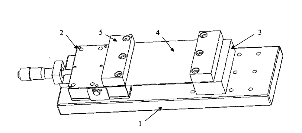
[0035] Refer to attached figure 1 , a test device for performance degradation caused by transistor lattice deformation, including five parts: 1 is a base, 2 is a precision displacement platform, 3 is a spacer, 4 is a carrier, and 5 is a pressing block. in,

[0036]The cuboid base 1 is located at the bottom of the device, and one end is provided with two rows and two columns of four screw holes, which are connected with the precision displacement platform 2 on it with screws; the other end is provided with four rows and three columns of twelve screw holes. When the invention fixes the spacer 3, it can be connected with the spacer 3 on it with screws through one row of screw holes according to the specific lattice deformation test requirements. In the embodiment of the present invention, the spacer 3 is fixed on a row of screw holes on the side closest to the precise displacement platform 2 with screws.

[0037] The precision displacement platform 2 is located on the upper lef...


PUM


Abstract

The invention discloses a device and method for testing performance degradation caused by transistor lattice deformation. The device for testing the performance degradation caused by the transistor lattice deformation comprises a base, a precise displacement platform, a cushion block, a carrier and a pressing block. The method for testing the performance degradation caused by the transistor lattice deformation comprises the following steps of (1) thinning a chip; (2) cutting the chip; (3) sticking the chip; (4) leading an electrode out of a transistor; (5) fixing the carrier; (6) testing the transistor before applying the stress; (7) applying the mechanical stress onto the chip; (8) testing the transistor under the stress; (9) judging whether the performance of the transistor degrades; and (10) obtaining the lattice deformation value when the performance of the transistor degrades. The device and method for testing the performance degradation caused by the transistor lattice deformation has the advantages of easily applying compression stress onto the chip, and being large in range of the applicable mechanical stress, good in chip bend uniform, simple and accurate in lattice tension amount calculation, and is suitable for analyzing the influence of the transistor lattice deformation on the performance of the transistor.

Description

technical field [0001] The invention belongs to the technical field of microelectronics, and further relates to a testing device and a method for performance degradation caused by lattice deformation of transistors in the technical field of semiconductor testing. The invention can be used for gallium nitride (Gallium Nitride, GaN) High Electron Mobility Transistors (High Electron Mobility Transistors, HEMTs) and other semiconductor transistor lattice deformation to cause performance degradation test, provide for the influence of transistor lattice deformation on transistor performance A more intuitive and convenient analysis method was developed. Background technique [0002] During the working process of transistors, the generation of lattice deformation will lead to the degradation of transistor performance. This effect is more pronounced for gallium nitride high electron mobility transistors and other semiconductor devices with piezoelectric effect. Therefore, it is ver...

Claims


Application Information

Patent Timeline
Patent Type & Authority Applications(China)
IPC IPC(8): G01R31/26
Inventor 马晓华陈伟伟郝跃祝杰杰侯斌
Owner 云南凝慧电子科技有限公司
Why Eureka
Try Eureka