Light beam imaging device

A beam imaging and light wave technology, applied in electrical components, circuits, semiconductor devices, etc., can solve the problems of high light wave transmission loss and single function

Active Publication Date: 2019-03-08
CHINA SCI PHOTON CHIP HAINING TECH CO LTD
View PDF11 Cites 2 Cited by
  • Summary
  • Abstract
  • Description
  • Claims
  • Application Information

AI Technical Summary

Problems solved by technology

[0004] In view of this, the embodiment of the present invention provides a beam imaging device to solve the problem of high transmission loss of light waves due to limitations of materials and other factors in the prior art, and the existing beam imaging device can only be used to transmit external equipment input The light wave, a technical problem with a single function

Method used


Image

  • Light beam imaging device
  • Light beam imaging device
  • Light beam imaging device

Examples


Embodiment Construction

[0023] In order to make the purpose, technical solutions and advantages of the embodiments of the present invention clearer, the technical solutions in the embodiments of the present invention will be clearly and completely described below in conjunction with the drawings in the embodiments of the present invention. Obviously, the described embodiments It is a part of embodiments of the present invention, but not all embodiments. Based on the embodiments of the present invention, all other embodiments obtained by those skilled in the art without making creative efforts belong to the protection scope of the present invention.

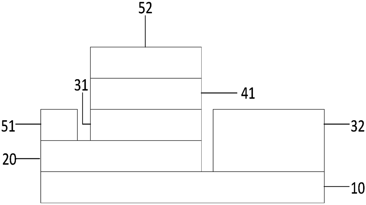
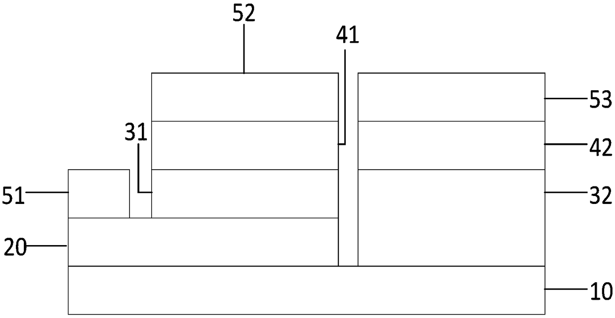
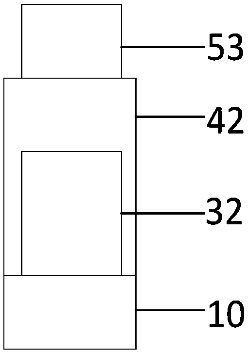
[0024] An embodiment of the present invention provides a beam imaging device, such as figure 1 As shown, the beam imaging device includes: a substrate layer 10; at least one light wave generating unit is arranged above the substrate layer 10 and is in contact with the substrate layer 10. The light wave generating unit includes a first type conductive lay...


PUM

PropertyMeasurementUnit
Bandgap widthaaaaaaaaaa
Refractive indexaaaaaaaaaa

Abstract

The invention discloses a light beam imaging device. The light beam imaging device comprises a substrate layer, at least one light wave generating unit and at least one second graphical layer, whereinthe at least one light wave generating unit is arranged above the substrate layer and is in contact with the substrate layer, each light wave generating unit comprises a first type of conducting layers, a first electrode layer and a first graphical layer which are arranged in a laminated manner in sequence, a second type of conducting layers and a second electrode layer, the graphical layer is used for compounding carriers of the first type of conducting layers and carriers of the second type of conducting layers, generating light waves and transmitting the light waves; the at least one second graphical layer and at least one light wave generating unit are arranged above the substrate layer at an interval, and are in contact with the substrate layer. The light beam imaging device providedby the embodiment of the invention can realize multiple functions of generating the light waves, transmitting the light waves, modulating the light waves and the like when different electrode layersare connected to a power supply; and moreover, the second graphical layer is arranged on the substrate layer, the second graphical layer can be used for transmitting the light waves, when the second graphical layer is directly formed on the substrate layer, the difficulty of film formation is reduced, and the transmission loss is reduced.

Description

technical field [0001] The invention relates to the technical field of semiconductors, in particular to a beam imaging device. Background technique [0002] The beam imaging device is the core part of lidar, which has excellent application advantages in automotive driverless and security environment monitoring. Traditional beam imaging devices generally use prisms, which is not conducive to integration. In the existing beam imaging device, a semiconductor integrated circuit is used instead of the prism device, which has the advantages of small size, low price and easy integration. [0003] However, in the process of transmitting light beams, due to the limitations of materials and other factors, the existing beam imaging devices have high transmission loss of light waves, and the existing beam imaging devices can only be used to transmit light waves input by external equipment, and have a single function. Contents of the invention [0004] In view of this, the embodiment...

Claims


Application Information

Patent Timeline
IPC IPC(8): H01L33/14H01L33/40H01L33/00
CPCH01L33/0012H01L33/14H01L33/40
Inventor 田立飞刘敬伟姜磊
Owner CHINA SCI PHOTON CHIP HAINING TECH CO LTD
Why Eureka
Try Eureka