

Conductive film, touch panel, and display device
A conductive film and electrode technology, which is applied in the input/output process of electrical digital data processing, instruments, and data processing, etc., can solve the problem of low periodicity, and achieve the effect of suppressing quality degradation
- Summary
- Abstract
- Description
- Claims
- Application Information
AI Technical Summary
Problems solved by technology
Method used
Image

Examples
no. 1 Embodiment approach
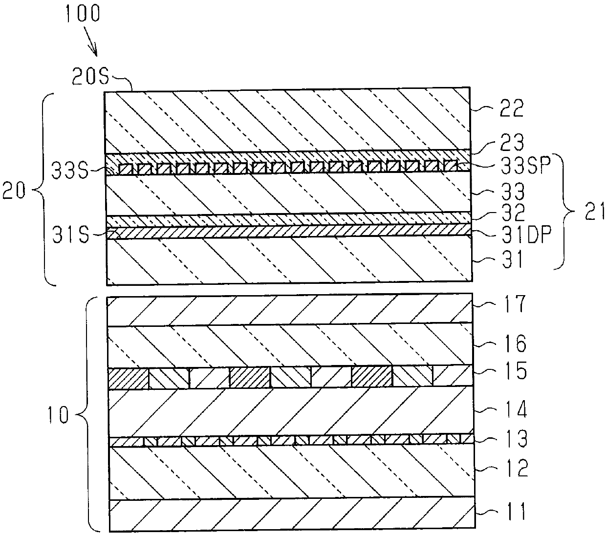
[0075] refer to Figure 1 to Figure 12 A first embodiment of a conductive film, a touch panel, and a display device will be described. In addition, each figure is a figure which schematically shows the structure of these conductive films, a touch panel, and a display device in order to demonstrate the 1st Embodiment, and the ratio of the size of each part which the structure shown in each figure has differs from an actual one in some cases. ratios are different.
[0076] [Configuration of display device]
[0077] refer to figure 1 The configuration of the display device will be described.
[0078] Such as figure 1 As shown, the display device 100 includes a laminated body in which a display panel 10, which is a liquid crystal panel, and a touch panel 20 are bonded together through a single transparent adhesive layer (not shown), and further includes a circuit for driving the touch panel 20. and a control unit that controls driving of the touch panel 20 . In addition, t...
no. 2 Embodiment approach
[0178] refer to Figure 13 ~ Figure 15 Description will be given with reference to the second embodiment of the conductive film, touch panel, and display device. Hereinafter, the difference between the second embodiment and the first embodiment will be mainly described, and the same components as those in the first embodiment will be assigned the same reference numerals and their descriptions will be omitted.
[0179] [Sensing electrode wire group composition]
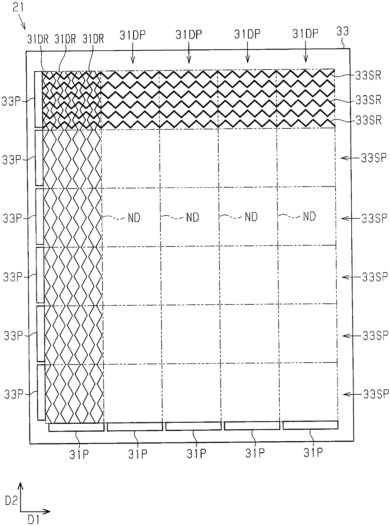
[0180] refer to Figure 13 The structure of the sensing electrode line 34SR of the second embodiment will be described. Such as Figure 13 As shown, the sensing electrode wire 34SR of the second embodiment has an irregular bending line shape, and is manufactured based on the regular bending line shape of the first embodiment.
[0181] In the sensing electrode line 34SR according to the second embodiment, the length Ls of the short line portion 33E is between the plurality of short line portions 33E arranged along t...
no. 3 Embodiment approach
[0216] refer to Figure 16 ~ Figure 21 A third embodiment of the conductive film, touch panel, and display device will be described. Hereinafter, the difference between the third embodiment and the first embodiment will be mainly described, and the same components as those in the first embodiment will be given the same reference numerals and their descriptions will be omitted.
[0217] [Sensing Electrode Composition]
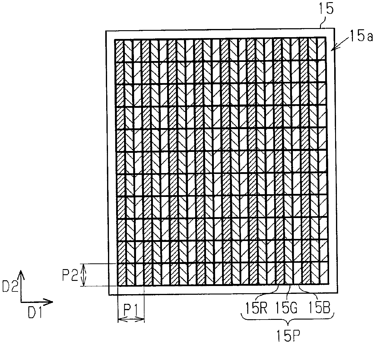
[0218] refer to Figure 16 Sensing electrode lines 63SR constituting sensing electrodes 33SP of the third embodiment will be described.
[0219] Such as Figure 16 As shown, each of the plurality of sensing electrode wires 63SR has a bent line shape extending in the first electrode direction D1 while repeatedly bending.
[0220] In detail, the sensing electrode line 63SR includes a plurality of bent portions 63Q and a plurality of straight line-shaped short line portions 63E connecting the bent portions 63Q adjacent to each other along the sensing electrode ...
PUM
 Abstract
Description
Claims
Application Information