Eureka AIR delivers breakthrough ideas for toughest innovation challenges, trusted by R&D personnel around the world.

Film forming apparatus, film forming method, and manufacturing method of electronic device

A film-forming device and film-forming method technology, applied in semiconductor/solid-state device manufacturing, electrical components, circuits, etc., can solve problems such as uneven film quality, no record of film-forming control, and film-forming quality reduction

Pending Publication Date: 2020-07-07
CANON TOKKI CORP
View PDF8 Cites 0 Cited by
  • Summary
  • Abstract
  • Description
  • Claims
  • Application Information

AI Technical Summary

Problems solved by technology

As a result, the quality of film formation may be reduced, such as film thickness, film quality unevenness, etc.
However, Patent Document 1 does not describe the control of film formation according to the pressure distribution of the sputtering gas in the chamber.

Method used


Image

  • Film forming apparatus, film forming method, and manufacturing method of electronic device
  • Film forming apparatus, film forming method, and manufacturing method of electronic device
  • Film forming apparatus, film forming method, and manufacturing method of electronic device

Examples


Embodiment approach 1

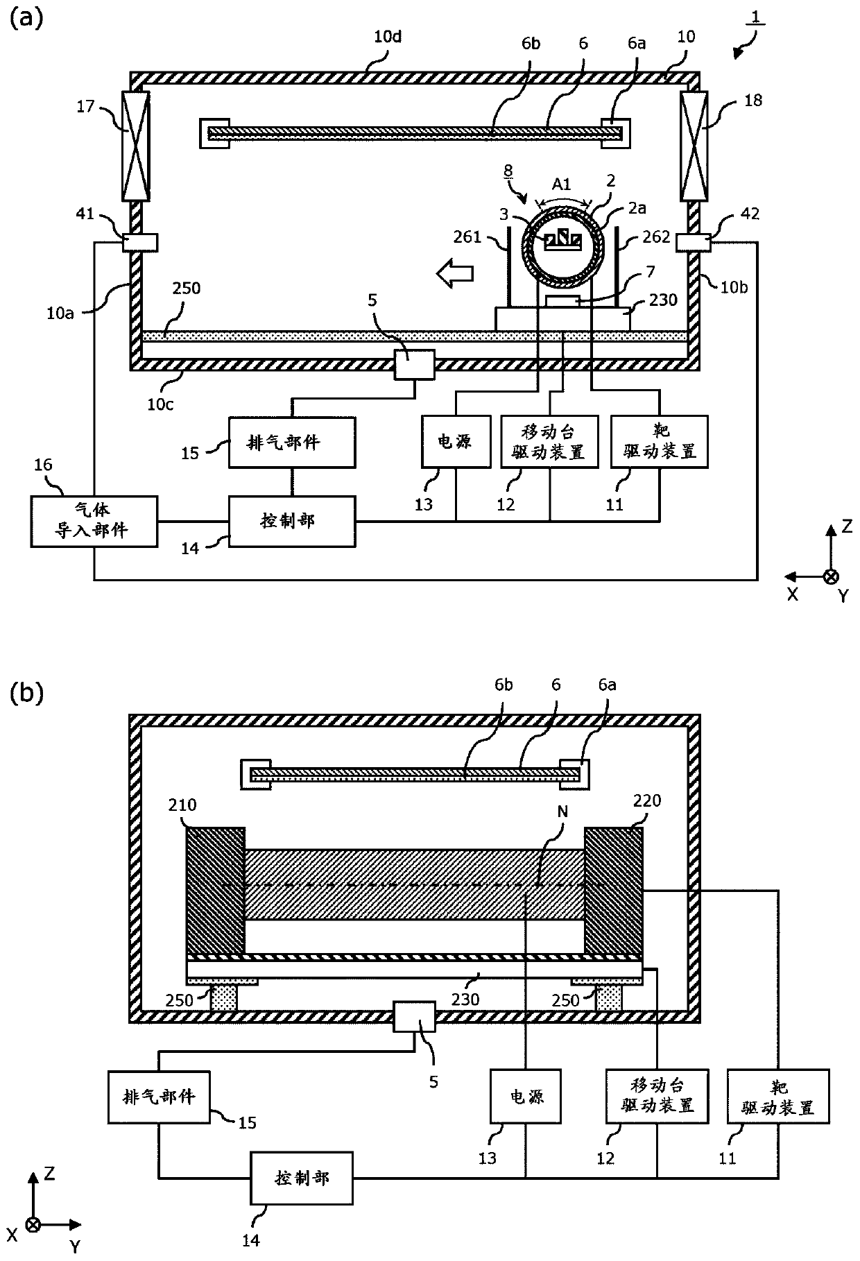
[0028] The basic configuration of the film forming apparatus 1 according to Embodiment 1 will be described with reference to the drawings. The film forming apparatus 1 is used to deposit and form a thin film on a substrate (including a structure in which a laminate is formed on the substrate) in the manufacture of various electronic devices such as semiconductor devices, magnetic devices, and electronic parts, and optical parts. More specifically, the film forming apparatus 1 is preferably used in the manufacture of electronic devices such as light emitting elements, photoelectric conversion elements, and touch panels. Among them, the film-forming apparatus 1 of the present embodiment is particularly preferably used in the production of organic light-emitting elements such as organic EL (Erectro Luminescence) elements, and organic photoelectric conversion elements such as organic thin-film solar cells. In addition, the electronic device in the present invention also includes a...

Embodiment approach 2

[0062] Next, Embodiment 2 of the present invention will be described. Hereinafter, differences from Embodiment 1 will be mainly described, and the same components will be given the same reference numerals to simplify the description.

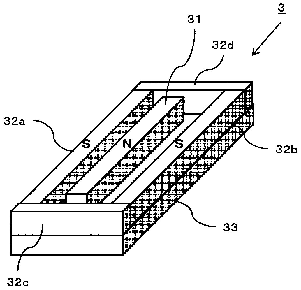
[0063] Figure 5 (a) shows the film formation apparatus 1 of this embodiment. In the film forming apparatus 1 , a planar cathode unit 308 using a flat plate-shaped target 302 is employed instead of a rotary cathode unit using a cylindrical target. The planar cathode unit 308 has a target 302 arranged parallel to the film formation object 6 , and the magnet unit 3 as a magnetic field generating member is arranged on the opposite side of the target 302 from the film formation object 6 . In addition, a backing plate 302 a to which power is applied from the power source 13 is provided on the surface of the target 302 opposite to the film formation object 6 . Sputtered particles are emitted from the sputtering region A1 by applying electric power ...

Embodiment approach 3

[0069] Next, Embodiment 3 of the present invention will be described. Hereinafter, differences from the above-described embodiments will be mainly described, and the same components will be given the same reference numerals to simplify the description.

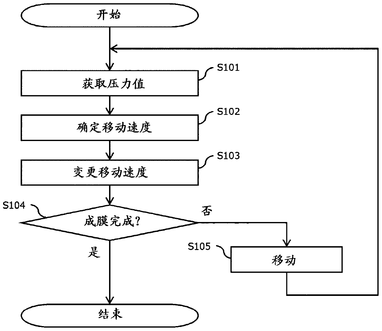
[0070] Image 6 The film formation apparatus 1 of this embodiment is shown. in the above Figure 5 (b)~ Figure 5 In (d), the magnet unit 3 in the planar cathode unit can move relative to the target 302 . In the present embodiment, the flat plate-shaped target 402 is larger than the film-forming object 6 in two directions of the X-axis direction and the Y-axis direction, and is fixedly installed with respect to the chamber 10 . In addition, the magnet unit 3 as a magnetic field generating member moves relative to the target 402 fixed to the chamber 10 (ie, relative to the chamber 10 ). Along with this, the sputtering region A1 of the target 402 from which the target particles are emitted also moves relative to the film fo...


PUM


Abstract

The invention provides a film forming apparatus, a film forming method, and a manufacturing method of an electronic device. According to the invention, even in the case where sputtering is performed while moving the sputtering area in a chamber having an uneven pressure distribution, it is possible to suppress deterioration in sputtering quality. The film forming device (1) has a chamber (10) in which the film-forming object (6) and the target (2) are arranged, and a movement member (movement table driving apparatus 12), which moves the sputtering area (A1) in which sputtered particles are generated from the target (2) in the chamber (10). The film forming apparatus (1) moves the sputtering area (A1) by a moving member while depositing sputtered particles on the film forming target (6) toform a film. The movement member changes the moving speed of the sputtering area (A1) according to the pressure near the sputtering area (A1).

Description

technical field [0001] The present invention relates to a film forming device, a film forming method and a method for manufacturing electronic devices. Background technique [0002] A sputtering method is widely known as a method for forming a thin film made of a material such as a metal or a metal oxide on a film formation object such as a substrate or a laminate formed on the substrate. A film-forming apparatus that forms a film by a sputtering method has a structure in which a target made of a film-forming material faces a film-forming object in a vacuum chamber. When a voltage is applied to the target, plasma is generated in the vicinity of the target, and sputter particles are released from the target surface by collision of ionized inert gas elements with the target surface, and the released sputter particles are deposited on the film formation object to form a film. Also known is a magnetron sputtering method in which a magnet is disposed on the back surface of the t...

Claims


Application Information

Patent Timeline
IPC IPC(8): C23C14/35C23C14/50C23C14/56H01L21/67
CPCC23C14/35C23C14/50C23C14/56H01L21/67011C23C14/34C23C14/54C23C14/3407C23C14/564H01J37/3417H01J37/3455H01J37/32844
Inventor 菅原洋纪松本行生
Owner CANON TOKKI CORP
Why Eureka
Eureka Blog
Learn More