Multi-camera circuit structure, terminal and computer readable storage medium

A circuit structure and multi-camera technology, applied in the field of camera circuits, can solve the problems of idle resource layout space, pressure, waste of cost, etc.

Inactive Publication Date: 2019-05-07
NUBIA TECHNOLOGY CO LTD
View PDF5 Cites 5 Cited by
  • Summary
  • Abstract
  • Description
  • Claims
  • Application Information

AI Technical Summary

Problems solved by technology

Two sets of completely independent camera modules cause all modules of the rear camera to be idle when the front camera is working, but when the user is actually using it, the front camera and the rear camera are not used at the same time, resulting in idle resources and Waste of layout space and pressure on cost

Method used


Image

  • Multi-camera circuit structure, terminal and computer readable storage medium
  • Multi-camera circuit structure, terminal and computer readable storage medium
  • Multi-camera circuit structure, terminal and computer readable storage medium

Examples


no. 1 example

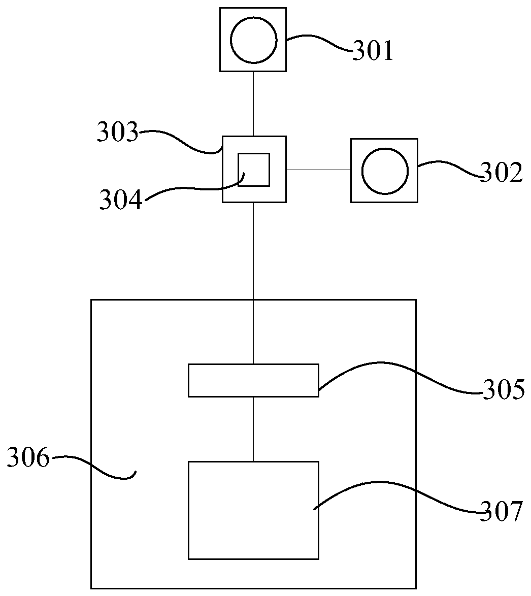
[0067] image 3 This embodiment provides a multi-camera circuit structure. The multi-camera circuit structure includes: a first image acquisition module 301, the first image acquisition module 301 is used to acquire a first image; a second image acquisition module 302, the second The image acquisition module 302 is used to collect the second picture image; the main body PCB303, the main body PCB303 is provided with a driver IC chip 304 for image processing, and the driver IC chip 304 is used to process the first picture image and / or the second picture image; the main body PCB303 Connected with the first image acquisition module 301 and the second image acquisition module 302, the first image acquisition module 301 and the second image acquisition module 302 are further connected with the drive IC chip 304 through the connection with the main body PCB303.

[0068] Such as image 3 Shown in image 3 The main body PCB303 is also connected to one end of the communication module 305 pr...

no. 2 example

[0082] This embodiment is a display example of the multi-camera circuit structure proposed in the embodiment of the present invention in an actual application scenario. We take a common dual-camera terminal with a front camera and a rear camera as an example for description.

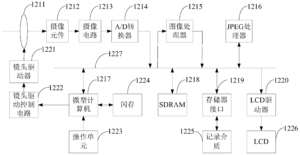
[0083] At present, the circuit structure of the common dual camera terminal is such as Figure 4 As shown, Figure 4 Among them, the front camera and the rear camera are both full-featured cameras. Each camera includes an image acquisition module, a main PCB and a driver IC chip. The driver IC chip is spot welded on the main PCB, and the main PCB is set in the image capture module. The rear of the camera is integrated with the image acquisition module; each camera must be connected to the motherboard PCB through a separate flexible circuit (FPC) and connector, and connected to the CPU on the motherboard PCB through the communication module on the motherboard PCB. Thus, the images collected by each camera are...

no. 3 example

[0089] This embodiment also provides a terminal, such as Image 6 As shown, the terminal includes a multi-camera circuit structure 60, a processor 61, a memory 62, a communication bus 63, and a display 64 proposed by the embodiment of the present invention; the communication bus 63 is used to implement the communication between the processor 61 and the memory 62 and the display 63 Connection communication; the processor 61 is used to transmit the image generated by the multi-camera circuit structure 60 to the display 64 and store the image in the memory 62 at the same time.

[0090] This embodiment also provides a computer-readable storage medium, where the computer-readable storage medium stores an image generated by the multi-camera circuit structure provided by the embodiment of the present invention.


PUM


Abstract

The invention discloses a multi-camera circuit structure. The invention discloses a terminal and a computer readable storage medium. The multi-camera circuit structure comprises: a First image acquisition module, a Second image acquisition module, the main body PCB and the driving IC chip arranged on the main body PCB; the first image acquisition module and the second image acquisition module areconnected with the main body PCB; The first image acquisition module and the second image acquisition module share the main body PCB and the driving IC, so that the problem that the main body PCB andthe driving IC in the cameras which do not work are in an idle state when one camera is in a working state in the existing multi-camera scheme is solved, and the cost of a plurality of camera assemblies is reduced. Meanwhile, only one set of main body PCB is connected with the mainboard PCB, and the communication module arranged on the mainboard is connected with the CPU, so that the number of thecommunication modules for communication between the camera in the multi-camera terminal and the CPU is reduced, and the difficulty and cost of circuit design are reduced.

Description

Technical field [0001] The present invention relates to the technical field of camera circuits, and more specifically, to a multi-camera circuit structure, a terminal and a computer-readable storage medium. Background technique [0002] The current smart phones are generally designed with front and rear dual cameras, and the layout and camera connector space are reserved for the front and rear cameras on the main PCB of the phone. The front camera and the rear camera are divided into two independent modules, with two independent photosensitive sensors and driver IC chips, and two independent FPCs and connectors to communicate with the main PCB board. Two sets of completely independent camera modules cause all the modules of the rear camera to be idle when the front camera is working, but when the user actually uses the front camera and the rear camera, they are not used at the same time, which results in the idleness and the opposite of resources. The waste of layout space and c...

Claims


Application Information

Patent Timeline
Patent Type & Authority Applications(China)
IPC IPC(8): H04N5/225H04N5/247H04N5/14
Inventor 王璟
Owner NUBIA TECHNOLOGY CO LTD
Why Eureka
Try Eureka