Semiconductor device and method of controlling said semiconductor device

a semiconductor device and semiconductor technology, applied in the direction of static storage, digital storage, instruments, etc., can solve the problems of inaccurate reading, circuit size cannot be reduced, and leakage current caused in unselected blocks at the time of reading or programming has become a problem, so as to reduce circuit size, accurate reading, and the effect of restricting leakage in unselected blocks

Active Publication Date: 2006-09-28
INFINEON TECH LLC
View PDF5 Cites 16 Cited by
  • Summary
  • Abstract
  • Description
  • Claims
  • Application Information

AI Technical Summary

Benefits of technology

[0025] The above objects of the present invention are also achieved by a method of controlling a semiconductor device including memory blocks each having groups of memory cells connected to word lines, and select gates selecting the groups of memory cells. This method includes the step of programming the select gates. In accordance with the present invention, data are stored in the select gates, so that the threshold value can be made higher than that of a regular transistor. In this manner, the select gates of unselected blocks can be certainly turned off, when predetermined voltages are applied to the gates. Accordingly, leakage in the unselected blocks can be restricted. Thus, accurate reading can be performed, and the circuit size can be reduced.
[0026] The above objects of the present invention are also achieved by a method of controlling a semiconductor device, including the steps of: precharging, at the time of reading data, a bit line running in memory blocks each having groups of memory cells connected to word lines, and select gates that select the groups of memory cells; and applying a back bias to the select gates of unselected blocks in a sensing period that follows a precharging period. In accordance with the present invention, the select gates can be certainly turned off, and leakage in the unselected blocks can be restricted. Thus, accurate reading can be performed, and the circuit size can be reduced. The method of the present invention further includes the steps of: erasing the memory cells of a selected block; and programming the select gates in the selected block having erased memory cells.
[0027] In accordance with the present invention, a semiconductor device that can perform accurate reading and has a smaller circuit size, and a method of controlling the semiconductor device can be provided.

Problems solved by technology

However, as higher integration and lower voltages are being achieved, leakage current caused in unselected blocks at the time of reading or programming has become a problem, as accurate reading cannot be performed.
Therefore, the circuit size cannot be reduced as the number of select gates becomes greater.

Method used


Image

  • Semiconductor device and method of controlling said semiconductor device
  • Semiconductor device and method of controlling said semiconductor device
  • Semiconductor device and method of controlling said semiconductor device

Examples


first embodiment

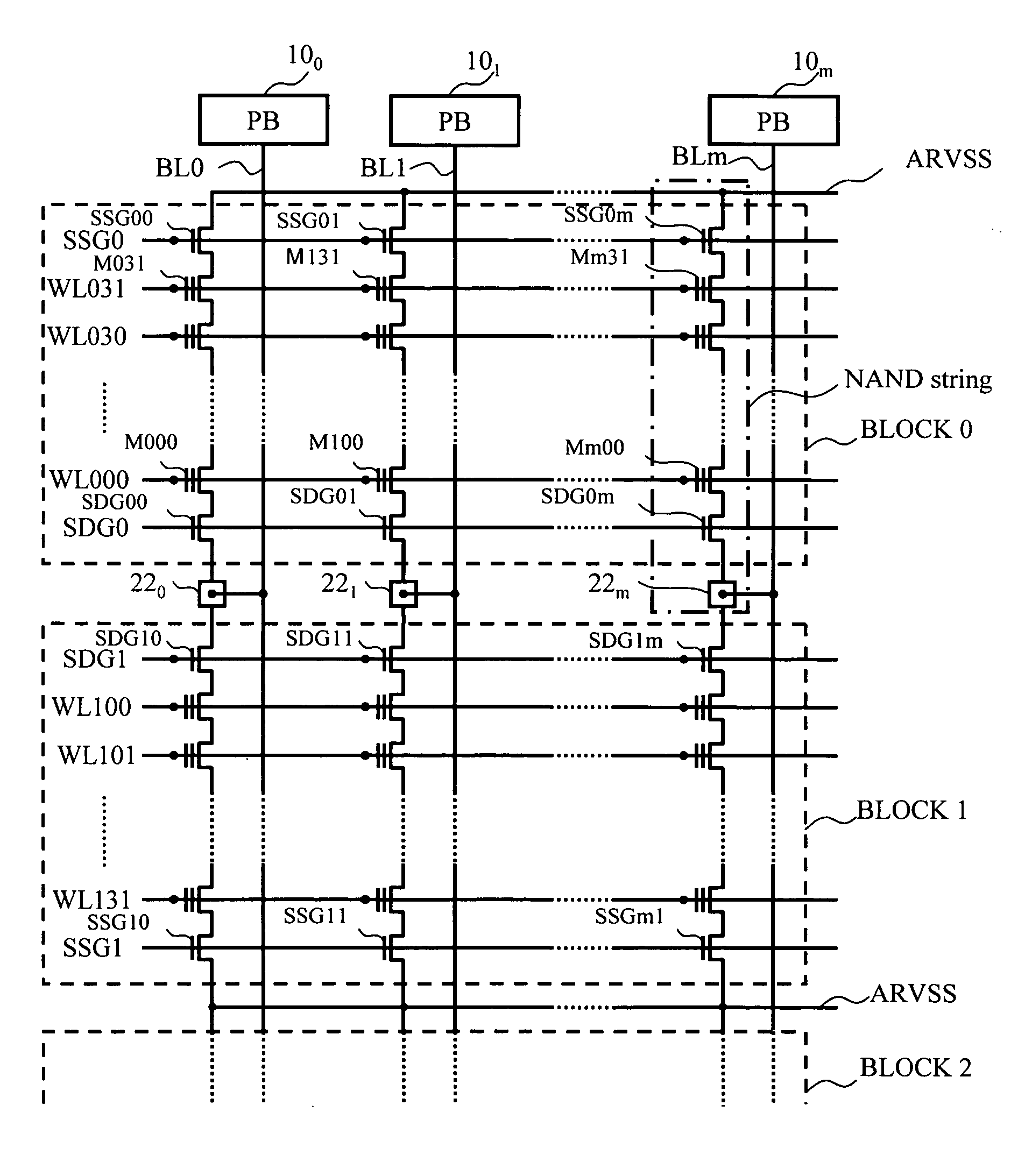
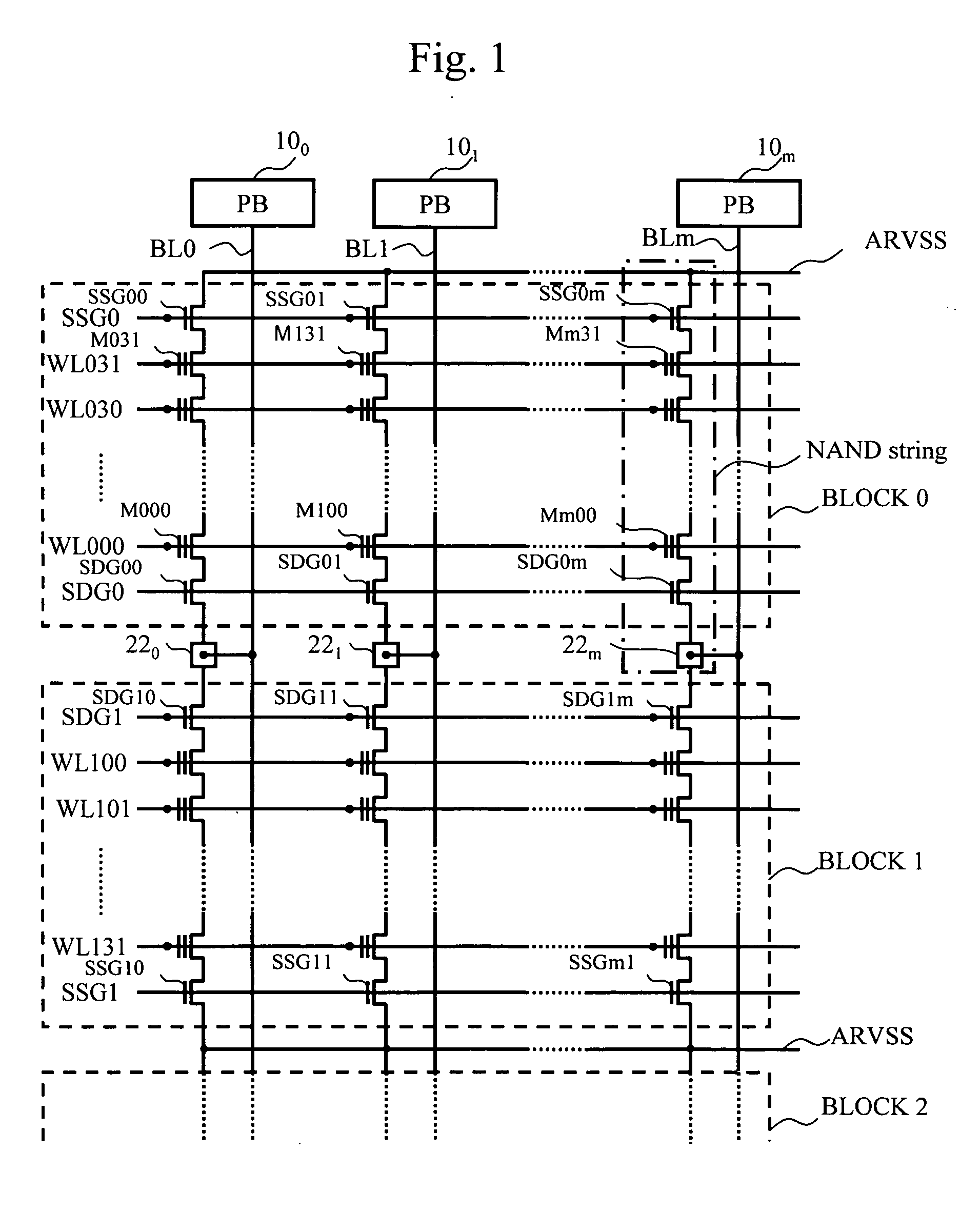
[0050]FIG. 5 is a block diagram of a NAND flash memory in accordance with a first embodiment of the present invention. The flash memory 51 includes a memory cell array 52, an I / O register buffer 53, an address register 54, a status register 55, a command register 56, a state machine 57, a high-voltage generating circuit 58, a row decoder 59, a page buffer 60, and a column decoder 61.

[0051] The memory cell array 52 has rewritable non-volatile memory cell transistors aligned with word lines WL and bit lines BL that are arranged in a matrix fashion.

[0052] The I / O register buffer 53 controls various signals and data corresponding to I / O terminals. The address register 54 temporarily stores address signals that are input through the I / O register buffer 53. The status register 55 temporarily stores status information. The command register 56 temporarily stores operation commands that are input through the I / O register buffer 53.

[0053] The state machine 57 controls the operation of each...

second embodiment

[0064] Next, a second embodiment of the present invention is described. FIG. 9 illustrates a FG-type NAND flash memory array and sense voltage conditions for reading in accordance with the second embodiment. Table 2 shows the conditions for reading in a selected block and an unselected block in the second embodiment.

TABLE 2UNSELECTEDBLOCKSELECTED BLOCK (BLOCK 0)(BLOCK 1)Sel WLUnsel WLSDGSSGWLSDGSSGARVSSBLPre-chargeVpass(4 V)Vpass(4 V)Vpass(4 V)0 VFloating0 V0 V0 V1 VSenseVread(0 V)Vpass (4 V)Vpass (4 V)VccFloating0 V0 V0 Vsensed

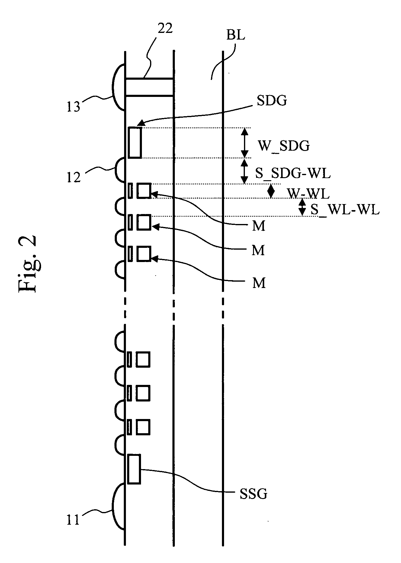
[0065] In FIG. 9, reference numeral 152 indicates a memory cell array, and reference numeral 60m indicates a page buffer. Thirty-two FG-type memory cells are connected in series, so as to form a NAND string. A select drain gate SDG0m and a select source gate SSG0m are connected to both ends of each NAND string. In FIG. 9, the block BLOCK0 is a selected block, and the block BLOCK1 is an unselected block.

[0066] The second embodiment is characterized in that ...

third embodiment

[0074] Next, a third embodiment of the present invention is described. FIG. 13 illustrates the array structure of a SONOS-type NAND flash memory in accordance with the third embodiment. In FIG. 13, reference numeral 252 indicates the memory cell array, and 60m indicates a page buffer. Sixteen SONOS-type memory cells are connected in series, so as to form a NAND string. A select drain gate SDG0m and a select source gate SSG0m are connected to both ends of each NAND string. The select drain gates SDG are also of a SONOS type. The select drain gate SDG0m is further connected to the bit line BLm via a drain contact 22m, and the bit line BLm is connected to the page buffer 60m. The block formed with m (m being 512 bytes+16 bytes) of NAND strings forms one erasing unit.

[0075] The m of memory cells that are connected to one word line WL form one page that is an access unit for reading and programming. Accordingly, reading and programming can be performed simultaneously on the m of memory ...


PUM


Abstract

A semiconductor device includes: memory blocks each having groups of memory cells that are connected to word lines; select gates for selecting the groups of memory cells; and an apply circuit that applies, at the time of reading data, a back bias to the select gates of unselected memory blocks.

Description

CROSS REFERENCE TO RELATED APPLICATIONS [0001] This is a continuation of International Application No. PCT / JP2004 / 017808, filed Nov. 30, 2004. BACKGROUND OF THE INVENTION [0002] 1. Field of the invention [0003] The present invention relates to a semiconductor device and a method of controlling the semiconductor device. [0004] 2. Description of the Related Art [0005] NAND flash memories and AND flash memories are widely used as flash memories for storing data. Examples of NAND flash memories that have floating gates (FG) as charge accumulation layers are disclosed in Japanese Unexamined Patent Publication No. 2001-308209 and Japanese Laid-Open Patent Application No. 2001-518696. [0006]FIG. 1 illustrates the array structure of a conventional FG-type NAND flash memory. In FIG. 1, WL000 through WL031 indicate word lines that are provided for one unit block, BLm indicates bit lines, and M indicates memory cells. The bit lines BLm are connected to page buffers 100 through 10m. Every thirt...

Claims


Application Information

Patent Timeline
Patent Type & Authority Applications(United States)
IPC IPC(8): G11C8/00
CPCG11C16/0466G11C16/0483G11C16/26G11C16/06
Inventor YANO, MASARUMURAKAMI, HIROKI
Owner INFINEON TECH LLC
Why Eureka
Try Eureka