Storage element, storage device, and signal processing circuit

a storage device and signal processing circuit technology, applied in the direction of instruments, sustainable buildings, and semiconductor/solid-state device details, can solve the problems of inconvenient data back up using the external storage device, the manufacturing process of the signal processing circuit is complex, and the data in the storage device cannot be erased accurately. , to achieve the effect of accurate reading and preventing data from being erased in the storage devi

Active Publication Date: 2012-07-05
SEMICON ENERGY LAB CO LTD
View PDF0 Cites 70 Cited by
  • Summary
  • Abstract
  • Description
  • Claims
  • Application Information

AI Technical Summary

Benefits of technology

[0044]In the second storage circuit, a signal held by the first capacitor is input to the gate of the second transistor. Therefore, after supply of the power supply voltage to the storage element is restarted, the signal held by the first capacitor can be converted into the one corresponding to the state (the on state or the off state) of the second transistor to be read from the second storage circuit. Consequently, an original signal can be accurately read even when a potential corresponding to the signal held by the first capacitor fluctuates to some degree.
[0045]By applying such a storage element to a storage device such as a register or a cache memory included in a signal processing circuit, data in the storage device can be prevented from being erased owing to the stop of the supply of the power supply voltage. Further, shortly after the supply of the power supply voltage is restarted, the storage element can return to the state before the power supply is stopped. Therefore, the power supply can be stopped even for a short time in the signal processing circuit or one or a plurality of logic circuits included in the signal processing circuit. Accordingly, it is possible to provide a signal processing circuit whose power consumption can be suppressed and a driving method of the signal processing circuit whose power consumption can be suppressed.

Problems solved by technology

In the case where data of a volatile storage device is stored in a nonvolatile storage device located in the periphery of the volatile storage device while the supply of the power supply voltage is stopped in a signal processing circuit, such a nonvolatile storage device is mainly formed using a magnetic element or a ferroelectric; thus, the manufacturing process of the signal processing circuit is complex.
In the case where data of the volatile storage device is stored in the external storage device while the supply of the power supply voltage is stopped in the signal processing circuit, it takes a long time for returning data from the external storage device to the volatile storage device.
Therefore, back up of data using the external storage device is not suitable in the case where the power supply is stopped for a short time so as to reduce power consumption.

Method used


Image

  • Storage element, storage device, and signal processing circuit
  • Storage element, storage device, and signal processing circuit
  • Storage element, storage device, and signal processing circuit

Examples


embodiment 1

[0085]A signal processing circuit includes a storage device. The storage device includes one or a plurality of storage elements which can store 1-bit data.

[0086]Note that the signal processing circuit of the preset invention includes, in its category, a CPU, a large scale integrated circuit (LSI) such as a microprocessor, an image processing circuit, a digital signal processor (DSP), or a field programmable gate array (FPGA), and the like.

(Structure of Storage Element)

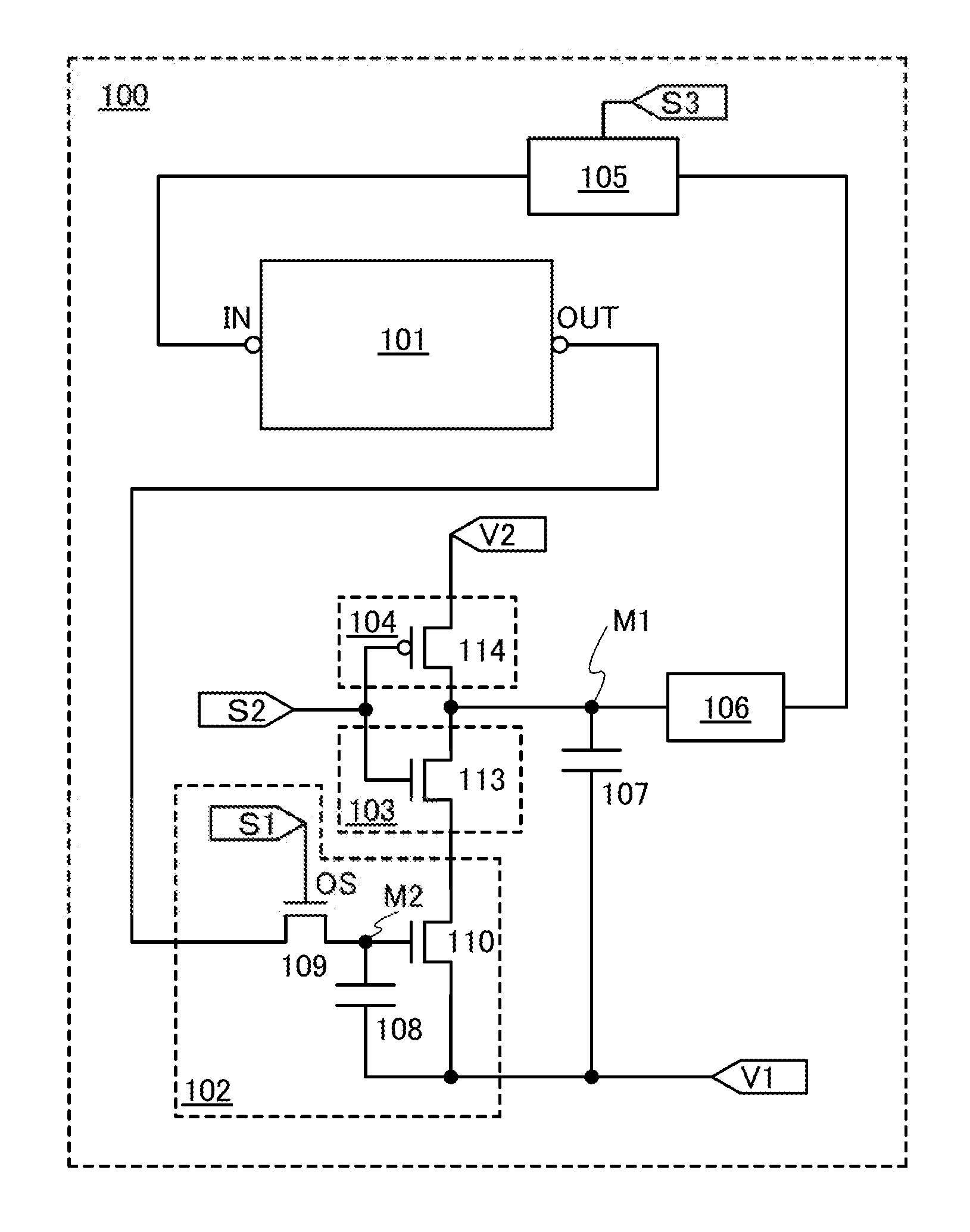
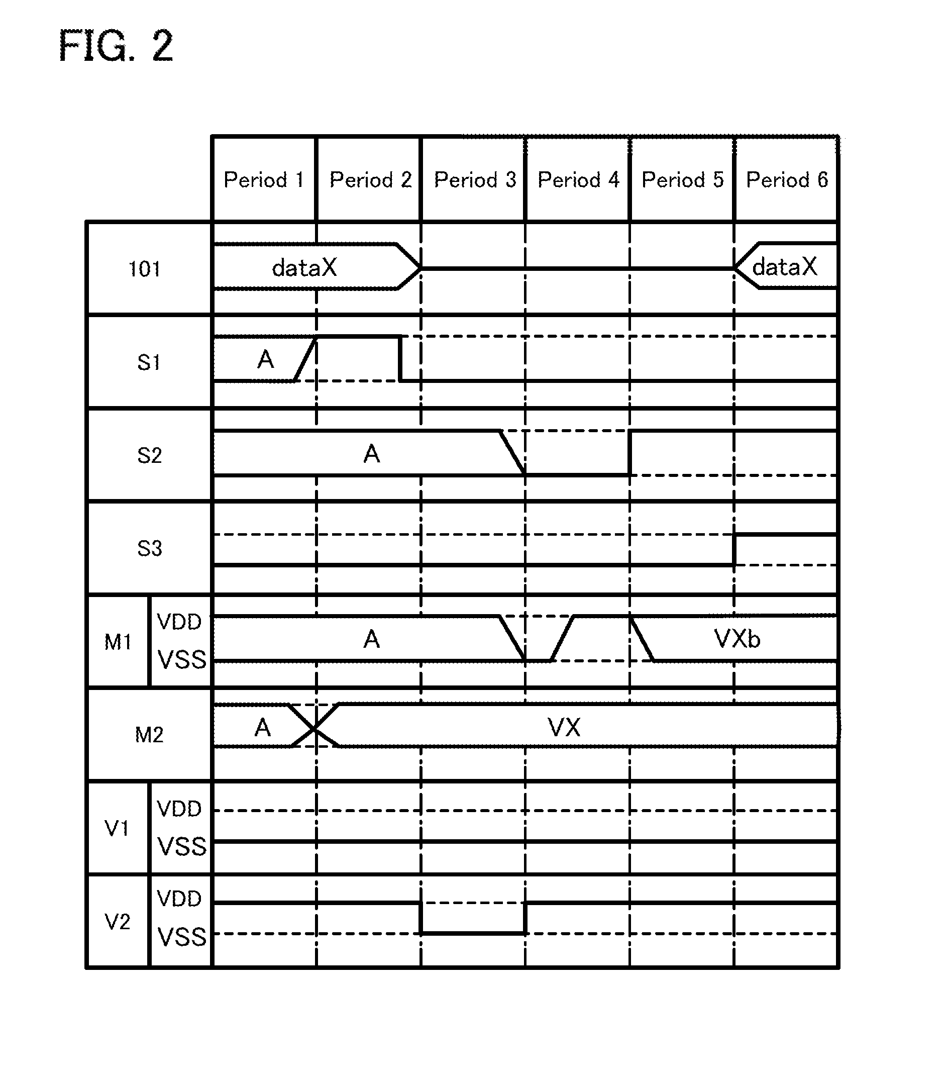
[0087]FIG. 1 is an example of a circuit diagram of a storage element. A storage element 100 includes a storage circuit 101, a storage circuit 102, a switch 103, a switch 104, a switch 105, a phase-inversion element 106, and a capacitor 107. The storage circuit 101 holds data only in a period during which a power supply voltage is supplied. The storage circuit 102 includes a capacitor 108, a transistor 109, and a transistor 110.

[0088]Note that the storage element 100 may further include another circuit element such as a...

embodiment 2

[0122]In this embodiment, a structure of a storage device including a plurality of storage elements described in Embodiment 1 will be described.

[0123]FIG. 3A illustrates a structural example of a storage device of this embodiment. The storage device illustrated in FIG. 3A includes a switching element 401 and a storage element group 403 including a plurality of storage elements 402. Specifically, as each of the storage elements 402, the storage element 100 whose structure is described in Embodiment 1 can be used. Each of the storage elements 402 included in the storage element group 403 is supplied with a high-level power supply potential VDD through the switching element 401. Further, each of the storage elements 402 included in the storage element group 403 is supplied with a potential of a signal IN and a low-level power supply potential VSS.

[0124]In FIG. 3A, a transistor is used for the switching element 401, and the switching of the transistor is controlled by a control signal S...

embodiment 3

[0128]In this embodiment, a structure of a signal processing circuit including the storage device described in Embodiment 2 or the storage element described in Embodiment 1 will be described.

[0129]FIG. 4 illustrates an example of a signal processing circuit according to one embodiment of the present invention. The signal processing circuit includes at least one or a plurality of arithmetic circuits and one or a plurality of storage devices. Specifically, a signal processing circuit 150 illustrated in FIG. 4 includes an arithmetic circuit 151, an arithmetic circuit 152, a storage device 153, a storage device 154, a storage device 155, a control device 156, and a power supply control circuit 157.

[0130]The arithmetic circuits 151 and 152 each include, as well as a logic circuit which carries out simple logic arithmetic processing, an adder, a multiplier, and various arithmetic circuits. The storage device 153 functions as a register for temporarily holding data when the arithmetic proc...


PUM


Abstract

A signal processing circuit whose power consumption can be suppressed is provided. In a period during which a power supply voltage is not supplied to a storage element, data stored in a first storage circuit corresponding to a nonvolatile memory can be held by a first capacitor provided in a second storage circuit. With the use of a transistor in which a channel is formed in an oxide semiconductor layer, a signal held in the first capacitor is held for a long time. The storage element can accordingly hold the stored content (data) also in a period during which the supply of the power supply voltage is stopped. A signal held by the first capacitor can be converted into the one corresponding to the state (the on state or off state) of the second transistor and read from the second storage circuit. Consequently, an original signal can be accurately read.

Description

BACKGROUND OF THE INVENTION[0001]1. Field of the Invention[0002]The present invention relates to a nonvolatile storage device which can keep a stored logic state even when power is turned off and also relates to a signal processing circuit including the nonvolatile storage device. Further, the present invention relates to driving methods of the storage device and the signal processing circuit. Furthermore, the present invention relates to an electronic device including the signal processing circuit.[0003]2. Description of the Related Art[0004]A signal processing circuit such as a central processing unit (CPU) has a variety of configurations depending on its application but is generally provided with some kinds of storage devices such as a register and a cache memory as well as a main memory for storing data or a program. A register has a function of temporarily holding data for carrying out arithmetic processing, holding a program execution state, or the like. In addition, a cache m...

Claims


Application Information

Patent Timeline
Patent Type & Authority Applications(United States)
IPC IPC(8): G11C11/24
CPCG11C11/24H01L29/26H01L27/108Y02B60/1225G11C19/184G06F1/3275H01L28/20H01L28/40Y02D10/00H01L27/0285H10B10/00H10B12/00H10B12/30H10B12/50H10B99/00G11C14/0009H01L29/24H01L29/7869H01L23/5226H01L27/0629
Inventor OHMARU, TAKUROENDO, MASAMI
Owner SEMICON ENERGY LAB CO LTD
Why Eureka
Try Eureka