Semiconductor device

a technology of semiconductors and devices, applied in the field of semiconductor devices, can solve the problems of large current consumption, inability to accurately carry out data readings, and voltage drop of power sources, and achieve the effects of reducing current consumption, accurate data readings, and high added valu

Inactive Publication Date: 2005-06-23
SEMICON ENERGY LAB CO LTD
View PDF13 Cites 70 Cited by
  • Summary
  • Abstract
  • Description
  • Claims
  • Application Information

AI Technical Summary

Benefits of technology

[0020] The semiconductor device of the invention comprising a data storage means and a power source control means enables reduction in current consumption and an accurate data reading. Furthermore, according to the semiconductor device of the invention comprising one or both of an address selection means having a selector circuit including a plurality of switches and an output bus, a first decoder circuit for selecting the switch in the selector circuit, and a second decoder circuit, and a display means having a plurality of pixels, in addition to a data storage means and a power source control means, a multifunctional semiconductor device with high added value can be provided.

Problems solved by technology

Thus, the conductive state between each source electrode and each drain electrode of the plurality of transistors at the same time results in an unnecessary current flowing to the power source line, leading to a large current consumption.
In addition, when a current consumption is increased, voltage drop of a power source may occur and accurate data reading may not be carried out.

Method used


Image

  • Semiconductor device
  • Semiconductor device
  • Semiconductor device

Examples


embodiment mode 1

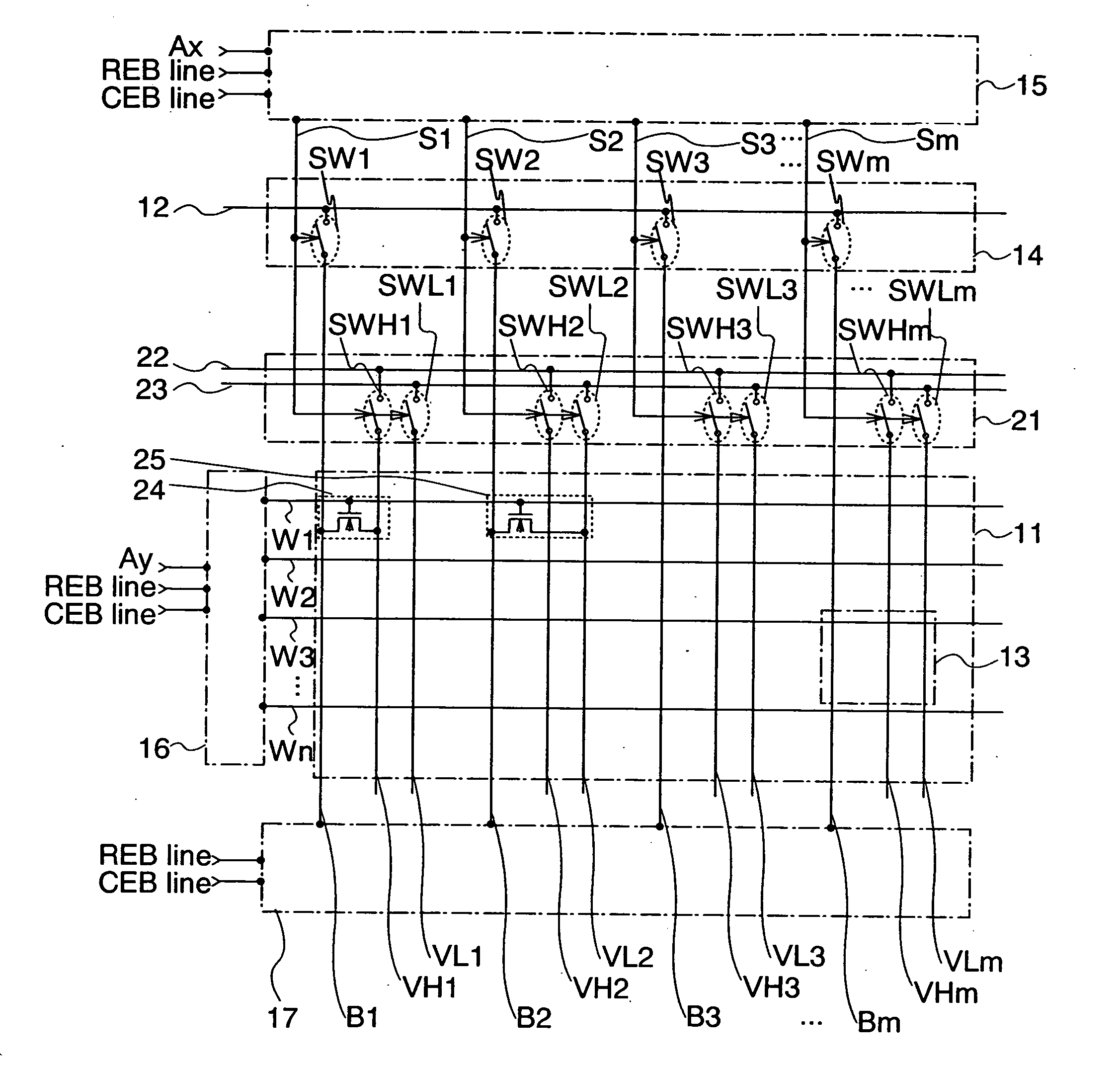
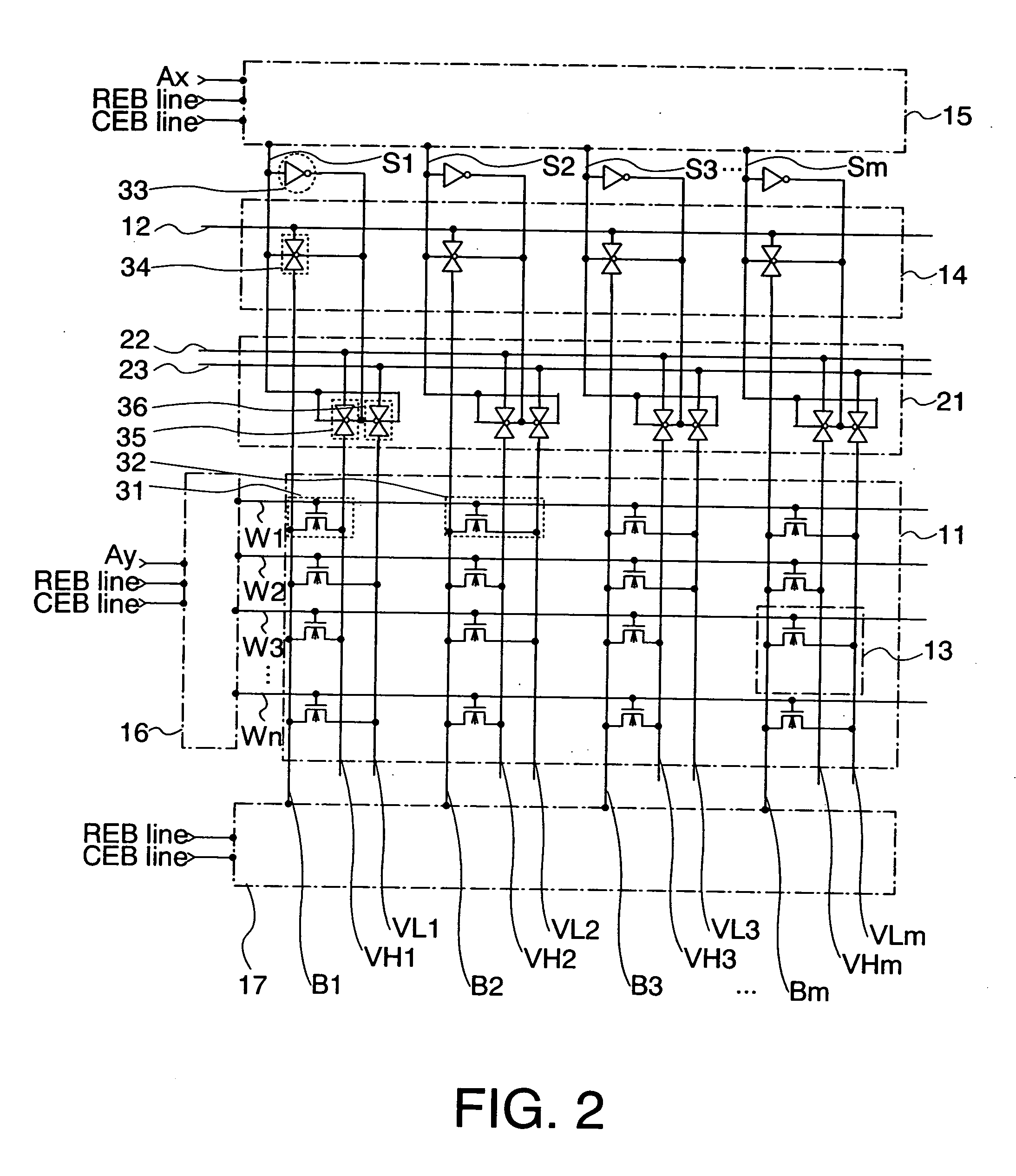
[0038] A semiconductor device having semiconductor elements according to the invention described below using FIG. 1. A semiconductor device including an ID tag comprises a data storage means (a memory cell array) 11 and a power source control means 21.

[0039] The data storage means (hereinafter referred to as a memory cell array) 11 has a plurality of memory cells 13 disposed in matrix. In addition, the memory cell array 11 has bit lines B1 to Bm (m is a positive integer) from a first column to an m-th column respectively and word lines W1 to Wn (n is a positive integer) from a first row to an n-th row respectively. In addition, the memory cell array 11 has first power source lines VH1 to VHm (m is a positive integer) and second power source lines VL1 to VLm (m is a positive integer) from the first column to the m-th column respectively. Each of the memory cells 13 includes a memory element in a region where the bit line Bx (1≦x≦n) and the word line Wy (1≦y≦m) cross each other throu...

embodiment mode 2

[0057] A panel which is an embodiment mode of a semiconductor device of the invention is described with reference to FIGS. 6A, 6B and 7. A panel comprises a substrate 406 over which a pixel portion 401 having a plurality of pixels, driver circuits 402 and 403 each including a plurality of transistors are formed (see FIG. 6A). Although the driver circuits 402 and 403 are integrally formed over the substrate 406, they may be attached or mounted on the substrate 406 by COG method as well. Thus, a display means corresponds to the pixel portion 401 only, or the pixel portion 401 and the driver circuits 402 and 403. The panel further comprises a memory means 404 such as a VRAM (Video Random Access memory), a RAM, or a ROM, and a CPU 405 over the substrate 406. In addition, the panel comprises an input terminal 409 for supplying a control signal of the driver circuits 402 and 403, the memory means 404, and the CPU 405 over the substrate 406. The input terminal 409 is supplied with signals ...

embodiment mode 3

[0062] The configuration of an ID tag (also referred to as an RFID tag, an IC tag, and an electronic tag) of the invention is described using FIGS. 8A to 8E below. An ID tag of the invention 306 has a semiconductor integrated circuit (IC chip) comprising a memory means 301, a control means 302, and a power source generation means 303, and an antenna 305 (see FIG. 8A). The semiconductor integrated circuit can be formed by a semiconductor element using a single-crystalline semiconductor substrate (e.g., a MOSFET, a bipolar transistor, and an inductor) or a semiconductor element using a semiconductor thin film (e.g., a TFT, an organic transistor, a diode, and an MIM element).

[0063] The configuration of a semiconductor device described in Embodiment Mode 1 is applied to the memory means 301. That is, the memory means 301 comprises the memory cell array and the power source control means. Accordingly, the ID tag 306 of the invention enables reduction in current consumption upon selectin...


PUM


Abstract

A semiconductor device in which a current consumption when a word line being selected is suppressed and accurate data reading is carried out. The semiconductor device of a semiconductor device of the invention comprises a data storage means and a power source control means. The data storage means has a plurality of memory cells. The power source control means has at least one power source line and a plurality of switches. In addition, the invention further comprises an address selection means having a selector circuit including a plurality of switches and an output bus, a first decoder circuit for selecting the switch in the selector circuit, and a second decoder circuit.

Description

BACKGROUND OF THE INVENTION [0001] 1. Field of the Invention [0002] The present invention relates to a semiconductor device having a semiconductor element. In addition, the invention relates to a semiconductor device which is capable of wireless data communication (hereinafter referred to as an ID tag). [0003] 2. Description of the Related Art [0004] In recent years, a semiconductor device having a semiconductor element has been applied to various fields such as an electronic apparatus including a high performance personal computer and a portable information terminal, an IC card, and an ID tag, and developed to have higher capacity in accordance with the achievement of a higher-speed operation of a CPU (Central Processing Unit) included in the electronic apparatus, increase in the amount of process data and the amount of store data in an IC card and the like. [0005] The semiconductor device having a semiconductor element as shown in FIG. 4 generally comprises a storage means (a memo...

Claims


Application Information

Patent Timeline
Patent Type & Authority Applications(United States)
IPC IPC(8): G11C16/08
CPCG11C16/08
Inventor SHIONOIRI, YUTAKAATSUMI, TOMOAKI
Owner SEMICON ENERGY LAB CO LTD
Why Eureka
Try Eureka