Data read circuit of solid-state imaging device, imaging apparatus, and data read method for solid-state imaging device

a solid-state imaging and data read circuit technology, applied in the direction of color signal processing circuits, color television details, television systems, etc., can solve the problems of increasing current consumption and deterioration of data read accuracy, increasing production costs of data read circuits, and taking a long time to perform data read operations, etc., to achieve convenient configuration and improve data read accuracy

Inactive Publication Date: 2006-08-03
SOCIONEXT INC
View PDF7 Cites 30 Cited by
  • Summary
  • Abstract
  • Description
  • Claims
  • Application Information

AI Technical Summary

Benefits of technology

[0016] However, temporary data signals outputted from the solid-state imaging devices are varied depending on the amount of exposure of the solid-state imaging device. Accordingly, the voltage of the inverting input terminal of the differential amplifier can be always maintained at a nearly constant level, which results in further improving the data read accuracy.
[0017] According to a preferable example of the aspect of the present invention, a counter of the measurement circuit initiates a count operation when the voltage of the ramp signal begins to vary. A measurement result output circuit of the measurement circuit acquires a counter value of the counter in response to the inversion of the output signal of the differential amplifier and outputs the acquired counter value as a digital value. Accordingly, a measurement circuit for measuring the amount of variation of the voltage of one of the input terminals to output a result of the measurement as the digital value can be easily configured.

Problems solved by technology

As a result, the production costs of the data read circuit are raised.
In addition, the increase of the number of the amplifiers causes the increase of the current consumption and the deterioration of data read accuracy.
Moreover, since the data read circuit disclosed in Japanese Unexamined Patent Application Publication No. 2002-218324 uses the chopper type voltage comparator in which a signal is transmitted from its input side to its output side via the capacitor, it may take a long time to perform a data read operation.
Therefore, such a data read circuit cannot be employed for an imaging apparatus having a number of pixels because the imaging apparatus requires a high-speed data read operation.

Method used


Image

  • Data read circuit of solid-state imaging device, imaging apparatus, and data read method for solid-state imaging device
  • Data read circuit of solid-state imaging device, imaging apparatus, and data read method for solid-state imaging device
  • Data read circuit of solid-state imaging device, imaging apparatus, and data read method for solid-state imaging device

Examples


Embodiment Construction

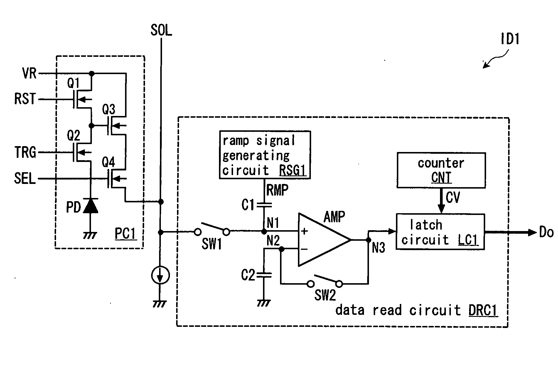
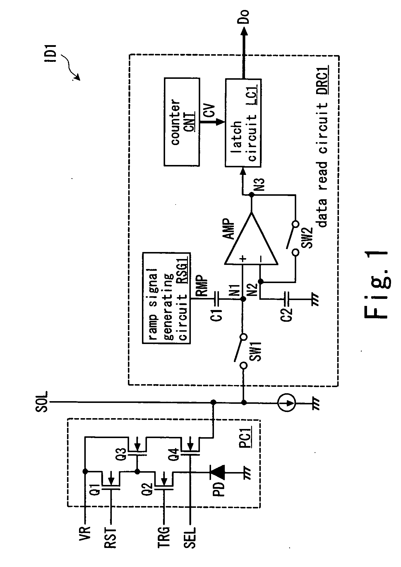
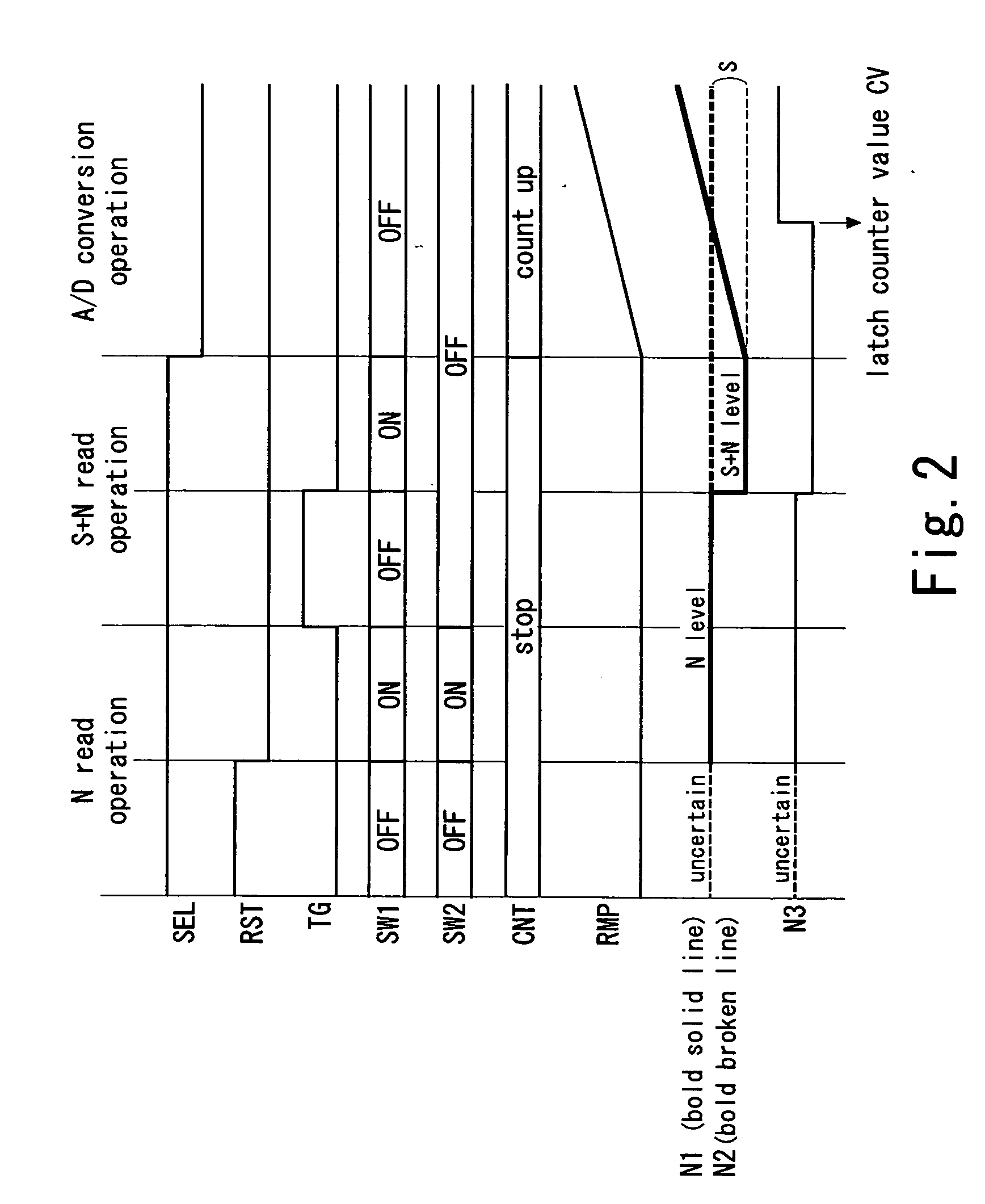
[0029] Hereinafter, exemplary embodiments of the present invention will be described with reference to the accompanying drawings. Signals depicted by a thick line refer to a plurality of signals. FIG. 1 shows a first embodiment of the present invention. An imaging apparatus ID1 of the first embodiment includes, for example, a data read circuit DRC1 having a plurality of pixel circuits PC1 provided for each of signal output lines SOL (columns) of pixel arrays arranged in a matrix.

[0030] Each pixel circuit PC1 (solid-state imaging device), which is a well-known four-transistor pixel circuit, has nMOS transistors Q1 to Q4 and a photodiode PD. The transistors Q1 and Q2 are connected in series between a reset voltage supply line VR and a cathode of the photodiode PD. A gate electrode of the transistor Q1 receives a reset signal RST. A gate electrode of the transistor Q2 receives a trigger signal TRG. An anode of the photodiode PD is connected to a ground line. The transistors Q3 and Q4 ...


PUM


Abstract

A differential amplifier has a first input terminal to which a voltage of a noise signal of the solid-state imaging device is supplied and a second input terminal to which a voltage of a temporary data signal having the noise signal of the solid-state imaging device superposed thereon is supplied. The differential amplifier inverts an output signal when a magnitude relationship in voltage between the first and second input terminals becomes reverse. A measurement circuit measures a variation amount of a voltage of the second input terminal from when the voltage of the second input terminal begins to vary in a direction to reverse the magnitude relationship to when the output signal of the differential amplifier is inverted, and outputs a measurement result as a digital value indicating a voltage of a real data signal obtained by removing the noise signal from the temporary data signal.

Description

CROSS REFERENCE TO RELATED APPLICATION [0001] This application is based upon and claims the benefit of priority from Japanese Patent Application No. 2005-027772, filed on Feb. 3, 2005, the entire contents of which are incorporated herein by reference. BACKGROUND OF THE INVENTION [0002] 1. Field of the Invention [0003] The present invention relates to a technique for reducing a scale of a data read circuit of a solid-state imaging device and current consumption of the data read circuit. [0004] 2. Description of the Related Art [0005] In general, an imaging apparatus has a data read circuit provided in each column of a pixel array. The data read circuit reads a noise signal and a data signal with the noise signal superposed thereon from a pixel circuit, generates a signal (an actual data signal) from which a common mode noise is removed by a CDS (Correlated Double Sampling) circuit, and converts the generated signal, which is an analog signal, into a digital signal using an ADC (Analo...

Claims


Application Information

Patent Timeline
Patent Type & Authority Applications(United States)
IPC IPC(8): H04N5/217H04N5/335H04N5/357H04N5/369H04N5/374H04N5/376H04N5/378
CPCH04N5/3575H04N5/378H04N25/616H04N25/75
Inventor HIGUCHI, TSUYOSHIFUNAKOSHI, JUNYAMAGATA, SEIJIMIZUGUCHI, TOSHITAKAYAMAMOTO, KATSUYOSHI
Owner SOCIONEXT INC
Why Eureka
Try Eureka