Semiconductor device and method of controlling the same

a technology of semiconductors and circuits, applied in the field of semiconductor devices, can solve the problems of low programming speed and large circuit size, and achieve the effect of shortening the writing time and reducing the circuit area

Active Publication Date: 2006-11-02
VALLEY DEVICE MANAGEMENT
View PDF8 Cites 16 Cited by
  • Summary
  • Abstract
  • Description
  • Claims
  • Application Information

AI Technical Summary

Benefits of technology

[0026] As described above, the present invention can provide a semiconductor device that requires a shorter writing

Problems solved by technology

Also, since the number of bits that can be programmed at one time is as small as several tens, the programming speed is low.

Method used


Image

  • Semiconductor device and method of controlling the same
  • Semiconductor device and method of controlling the same
  • Semiconductor device and method of controlling the same

Examples


Embodiment Construction

[0039] The following is a description of embodiments of the present invention, with reference to the accompanying drawings. In the following description, a flash memory having a NAND I / F formed with SONOS-type memory cells will be described. The features described below are applicable not only to SONOS-type cell arrays but also to FG-type cell arrays.

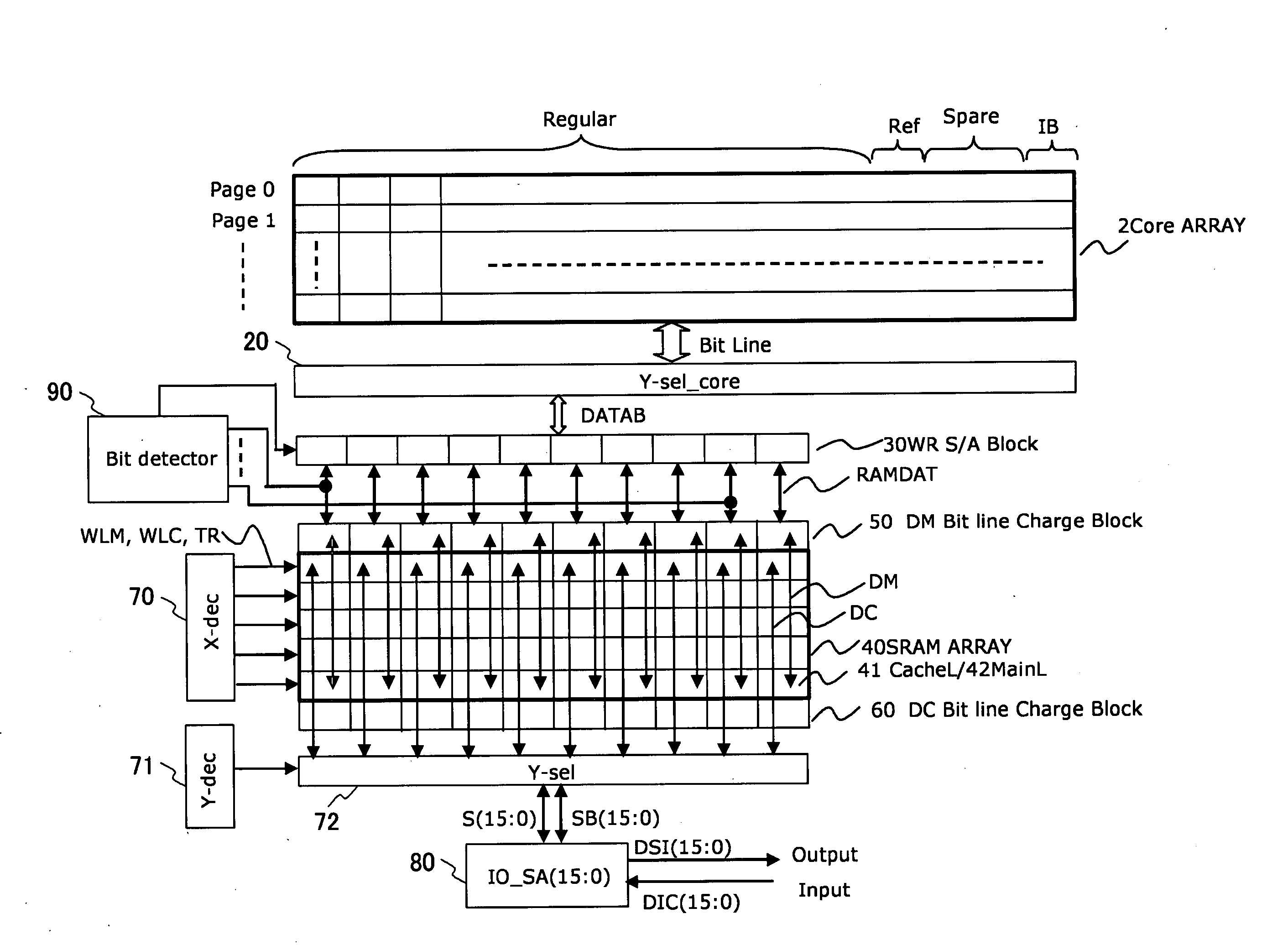
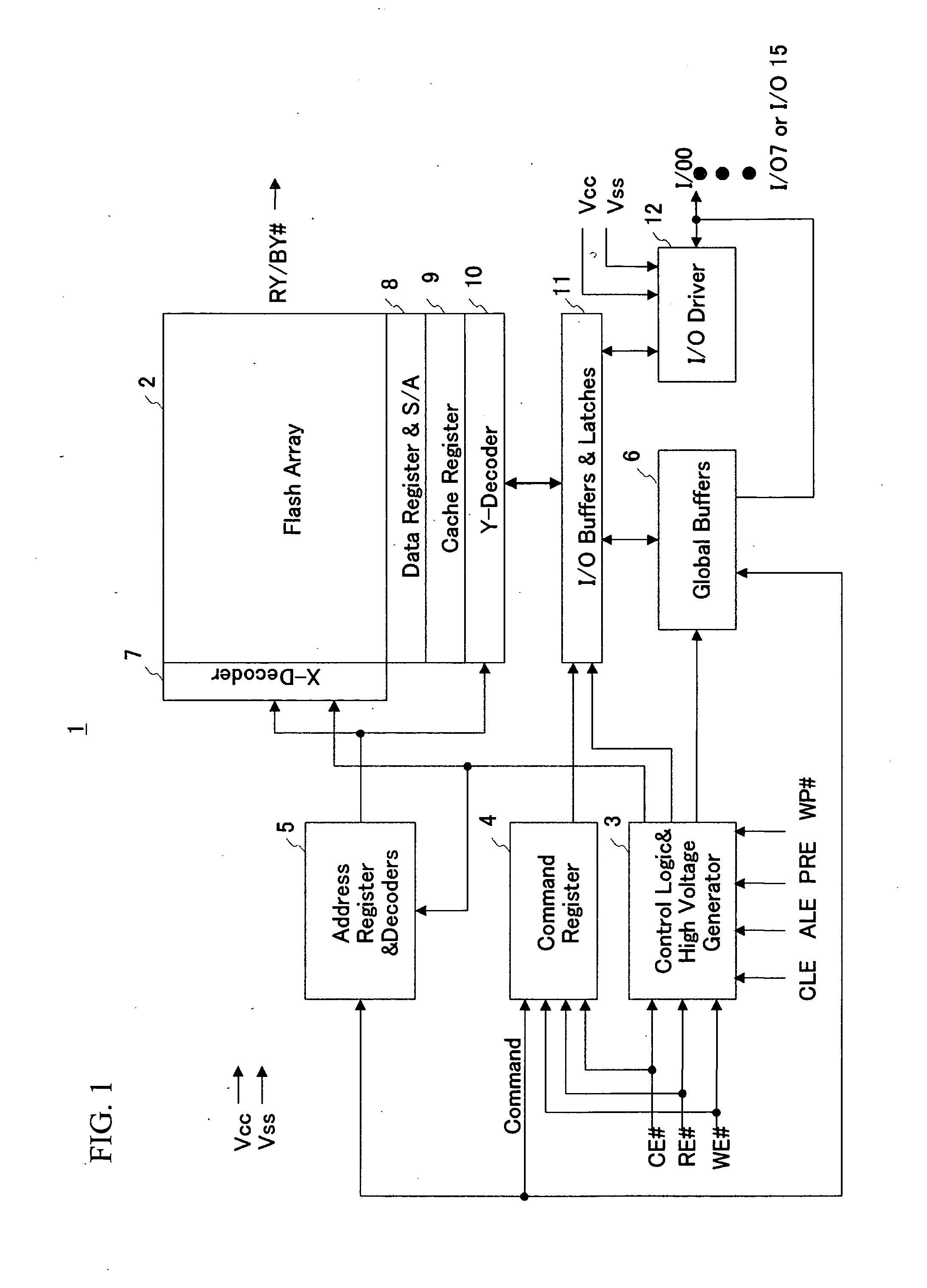
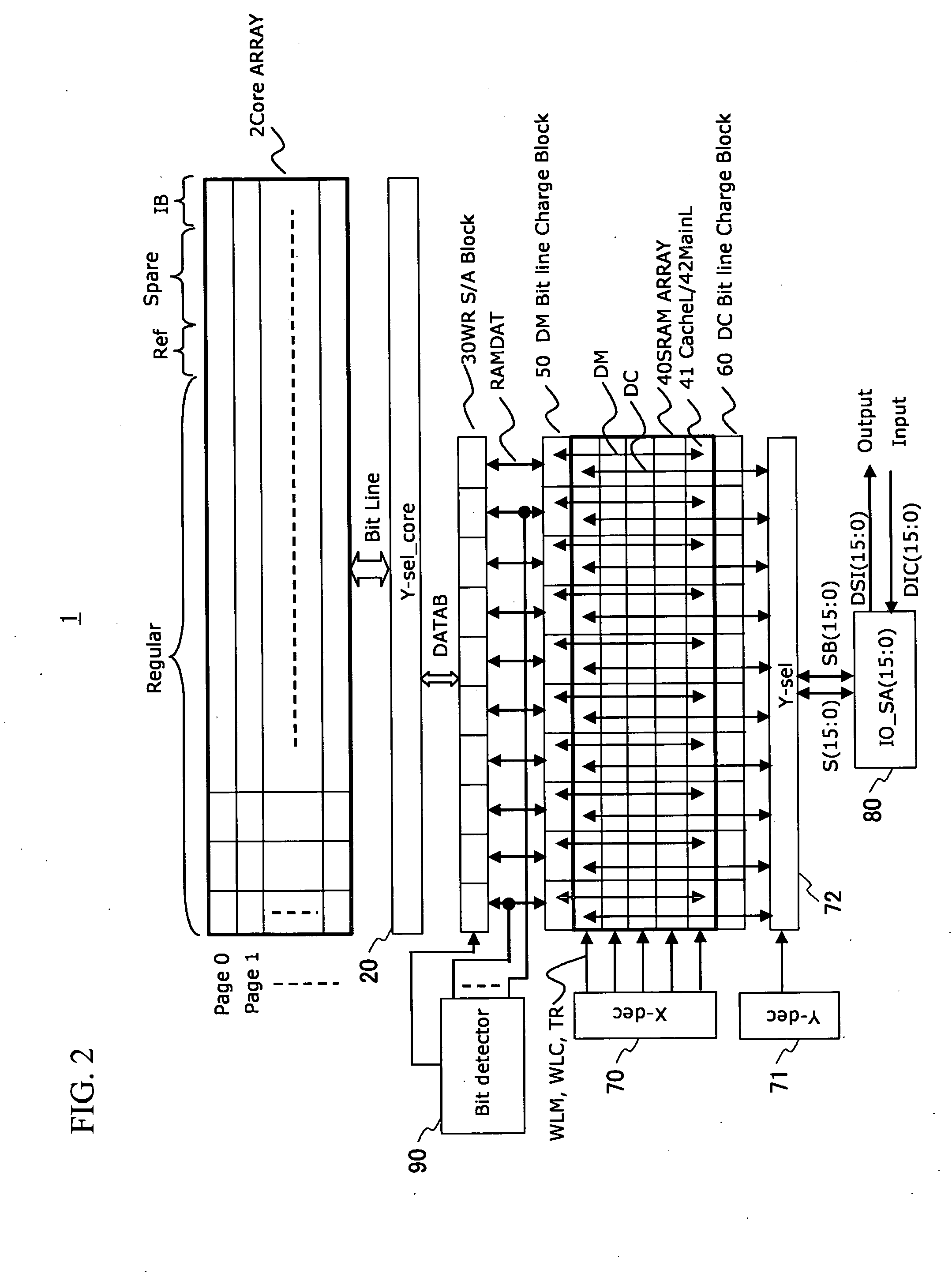
[0040]FIG. 1 is a block diagram of a flash memory 1. The flash memory 1 includes a memory cell array 2, a state machine and high-voltage generating circuit 3, a command register 4, an address register and decoder 5, a global buffer 6, an X-decoder 7, a data register and sense amplifier 8, a cache register 9, a Y-decoder 10, an I / O buffer and latch circuit 11, and an input / output driver 12.

[0041] The memory cell array 2 includes rewritable non-volatile memory cells that are arranged along word lines WL and bit lines BL in a matrix fashion. Each of the memory cells is a cell wherein the write function is performed through hot electron i...


PUM


Abstract

A semiconductor device (1) includes a non-volatile memory cell array (2), a write/read circuit (30) writing data into and reading data from the non-volatile memory cell array (2), a data input/output circuit (80), and a volatile memory cell array (40) including a first latch circuit (41) that is connected to the write/read circuit (30) and latches first data, and a second latch circuit (42) that is connected to the data input/output circuit (80) and latches second data. The device (1) may further include an inverter circuit (310) that inverts the first data in accordance with the number of bits to be actually written among the first data, and a control circuit (3) that causes the second data to be latched in the second latch circuit (42) while the first data is being written into the non-volatile memory cell array (2). This semiconductor device (1) has a shorter writing time and a smaller circuit area.

Description

CROSS-REFERENCES TO RELATED APPLICATIONS [0001] This is a continuation of International Application No. PCT / JP2005 / 06310, filed Mar. 31, 2005 which was not published in English under PCT Article 21(2).BACKGROUND OF THE INVENTION [0002] 1. Field of the Invention [0003] The present invention generally relates to a semiconductor device and a method of controlling such semiconductor device. [0004] 2. Description of the Related Art [0005] A NAND flash memory collectively performs write and read by “pages” (by two kilbyte (Kbyte) pages, for example). When writing, the data of one page is input from an I / O terminal (sixteen bits wide) to a page buffer in a serial fashion. In the page buffer, the latch circuits for one page are prepared for latching program data. When the data latch into the page buffer transfer is completed, programming is performed simultaneously on the subject memory cells. When reading, data is read in from the memory cells of one page, and the read data is collectively...

Claims


Application Information

Patent Timeline
IPC IPC(8): G11C14/00
CPCG11C16/10
Inventor YANO, MASARUARAKAWA, HIDEKISAKASHITA, MOTOTADA
Owner VALLEY DEVICE MANAGEMENT
Why Eureka
Try Eureka