Semiconductor device, display device and electronic device

a technology of display device and semiconductor, applied in the direction of diodes, digital storage, instruments, etc., can solve the problem of noise in the wiring for supplying current, and achieve the effect of shortening the write time of the signal

Active Publication Date: 2005-11-24
SEMICON ENERGY LAB CO LTD
View PDF52 Cites 15 Cited by
  • Summary
  • Abstract
  • Description
  • Claims
  • Application Information

AI Technical Summary

Benefits of technology

[0049] According to the invention, when a potential of a wiring through which a signal current flows when writing a signal to a current source circuit becomes outside a range of a potential of a normal operation, the potential can be set within the normal range rapidly. Therefore, a write time of a signal can be short.

Problems solved by technology

Here, noise may occur in a wiring for supplying a current.

Method used


Image

  • Semiconductor device, display device and electronic device
  • Semiconductor device, display device and electronic device
  • Semiconductor device, display device and electronic device

Examples


embodiment mode 1

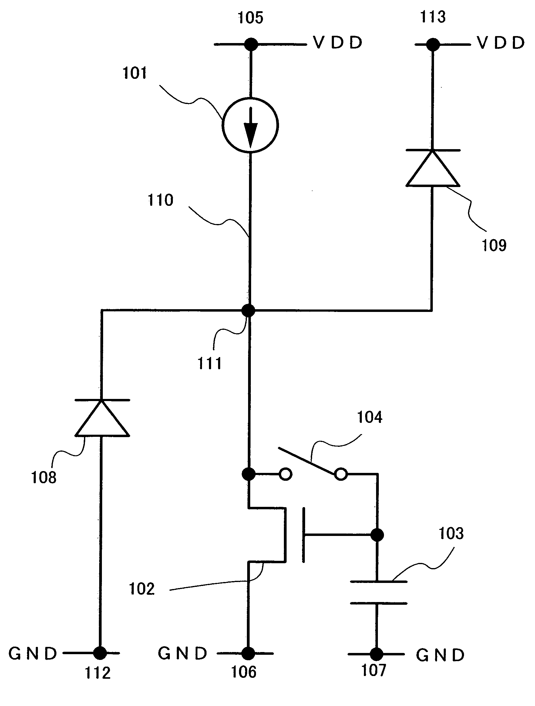
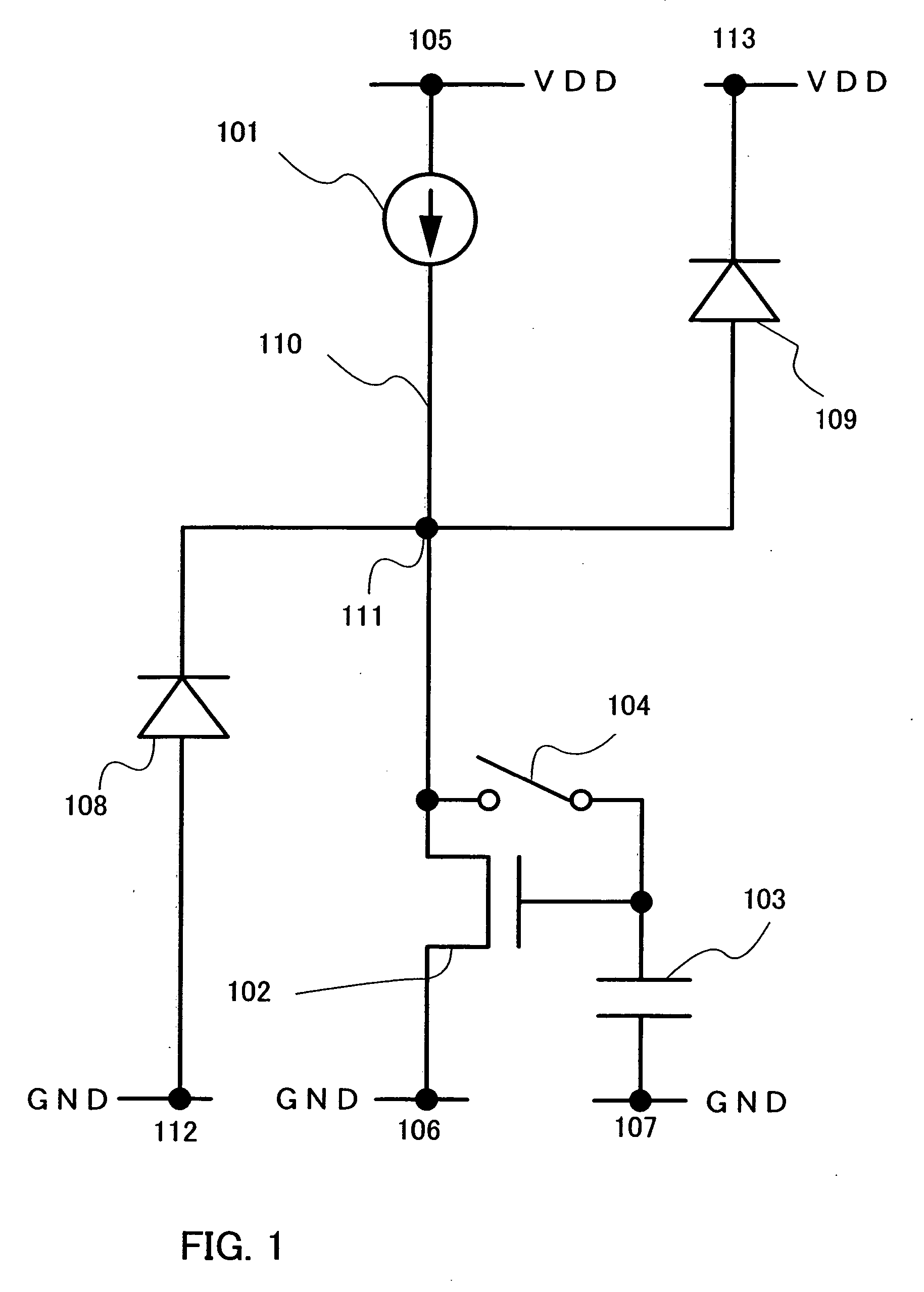
[0137] As the reference current source 101 in FIG. 1, a transistor which operates in the saturation region is often used. In this embodiment mode, a principle of the invention in the case of applying a transistor which operates in the saturation region to the reference current source 101 is described.

[0138]FIG. 4 shows a configuration of a current source circuit in the case of applying a transistor 401 which operates in the saturation region to the reference current source 101 shown in FIG. 1. A source terminal of the transistor 401 is connected to the wiring 105 and a drain terminal thereof is connected to the wiring 110. A gate terminal 402 of the transistor 401 is applied a predetermined potential. The transistor 401 operates in the saturation region, therefore, a current value is mostly determined by a potential difference between the gate terminal 402 and the source terminal and is not affected by a potential of the drain terminal.

[0139] That is to say, the source terminal ha...

embodiment mode 2

[0154] The structure described in Embodiment Mode 1 employs a P-channel transistor which functions as a reference current source, however, the invention is not limited to this. FIG. 9 shows an example of the case of changing the polarity (conductivity) of transistor which functions as a reference current source without changing the connection of the circuit with respect to the circuit shown in FIG. 4. It is to be noted in FIG. 9 that an N-channel transistor is employed as the reference current source 801 in FIG. 8.

[0155] A source terminal of a transistor 901 is connected to a wiring 805 while a drain terminal thereof is connected to a wiring 810. A gate terminal of the transistor 901 is inputted with a predetermined potential. The transistor 901 operates in the saturation region, therefore, a current value is mostly determined by a potential difference between the gate terminal 902 and the source terminal and is not affected by a potential of the drain terminal. That is to say, the...

embodiment mode 3

[0170] Another configuration of a current source circuit to which the invention can be applied is described. In a current source TFT of a current source circuit of this embodiment mode, a source terminal thereof is not connected to a fixed potential. In other words, the invention is applicable to a current source circuit having a configuration where a potential of the source terminal of the current source TFT changes like the configuration described in this embodiment mode.

[0171] First, a configuration of the current source circuit of this embodiment mode is shown in FIG. 35. One side of a wiring 3510 is connected to a wiring 3505 through a reference current source 3501. The other side of the wiring 3510 is connected to a source terminal of a transistor 3502 and then to a gate terminal thereof through a capacitor 3503. Further, the gate terminal of the transistor 3502 is connected to a drain terminal of the transistor 3502 and to a wiring 3506 through a switch 3504. Accordingly, th...


PUM


Abstract

When writing a signal current from a current source to a current source circuit, noise occurs in some cases in a wiring through which a current flows, which may cause a potential of the wiring to be outside the normal range. As the potential does not turn back within the normal range easily at this time, writing to the current source circuit is delayed. According to the invention, when the potential becomes outside the normal range due to noise occurring in a wiring through which a current flows when writing a signal current from a current source to a current source circuit, a current is supplied from other than the current source, thereby the potential of the wiring can turn back within the normal range rapidly.

Description

BACKGROUND OF THE INVENTION [0001] 1. Field of the Invention [0002] The present invention relates to a semiconductor device provided with a function to control a current supply to a load by a transistor. In particular, the invention relates to a semiconductor device including a pixel formed of a current driving light emitting element of which luminance changes according to current, and a signal driver circuit thereof. [0003] 2. Description of the Related Art [0004] In recent years, what is called a self-light emitting display device of which pixel is formed of a light emitting element such as a light emitting diode (LED) is attracting attentions. As a light emitting element used for such a self-light emitting display device, an organic light emitting diode (OLED), an organic EL element, an electroluminescence (EL) element and the like are attracting attentions and used for an organic EL display and the like. [0005] A light emitting element such as an OLED which is a self-light emitt...

Claims


Application Information

Patent Timeline
Patent Type & Authority Applications(United States)
IPC IPC(8): G09G3/20G11C7/00
CPCG09G3/325G09G3/3283G09G2300/0842G09G2300/0861H01L27/3276G09G2320/0209H01L27/0629H01L27/1255G09G2310/0262H10K59/131G09G2320/0233
Inventor KIMURA, HAJIMEYAMAZAKI, YU
Owner SEMICON ENERGY LAB CO LTD
Why Eureka
Try Eureka