Semiconductor Device and Electronic Device Including Semiconductor Device

a semiconductor and electronic device technology, applied in the direction of logic circuit coupling/interface arrangement, pulse technique, instruments, etc., can solve the problems of parasitic capacitance of transistors included in the shift register, gate and source of transistors are likely to be short-circuited, and the characteristic deterioration of pull-up transistors can be suppressed, and the channel width of transistors is smaller.

Active Publication Date: 2010-09-30
SEMICON ENERGY LAB CO LTD
View PDF28 Cites 43 Cited by
  • Summary
  • Abstract
  • Description
  • Claims
  • Application Information

AI Technical Summary

Benefits of technology

[0063]An embodiment of the present invention can suppress characteristic deterioration of a transistor. Alternatively, an embodiment of the present invention can make the channel width of a transistor smaller. In particular, characteristic deterioration of a pull-up transistor can be suppressed or the channel width of a pull-up transistor can be smaller. Alternatively, an embodiment of the present invention can make the amplitude of a signal larger. Alternatively, an embodiment of the present invention can make a time during which a transistor included in a pixel is on longer. Alternatively, an embodiment of the present invention can improve a shortage of writing to a pixel. Alternatively, an embodiment of the present invention can make a falling time of a signal shorter. Alternatively, an embodiment of the present invention can make a rising time of a signal shorter. Alternatively, an embodiment of the present invention can prevent a video signal for a pixel in a row from being written to a pixel in another row. Alternatively, an embodiment of the present invention can reduce variation of falling times of a signal. Alternatively, an embodiment of the present invention can make an influence of feedthrough on a pixel even. Alternatively, cross talk can be reduced. Alternatively, an embodiment of the present invention can make the area of layout smaller. Alternatively, an embodiment of the present invention can make a frame of a display device narrower. Alternatively, an embodiment of the present invention can make a display device have higher definition. Alternatively, an embodiment of the present invention can improve yield. Alternatively, an embodiment of the present invention can reduce costs. Alternatively, an embodiment of the present invention can reduce distortion of a signal. Alternatively, an embodiment of the present invention can reduce delay of a signal. Alternatively, an embodiment of the present invention can reduce power consumption. Alternatively, an embodiment of the present invention can reduce current supply capability of an external circuit. Alternatively, an embodiment of the present invention can reduce the size of an external circuit or the size of a display device including the external circuit.

Problems solved by technology

When the channel width of a transistor is larger, a gate and a source or a drain of the transistor are likely to be short-circuited.
Moreover, when the channel width of a transistor is larger, parasitic capacitance of transistors included in the shift register may be increased in some cases.

Method used


Image

  • Semiconductor Device and Electronic Device Including Semiconductor Device
  • Semiconductor Device and Electronic Device Including Semiconductor Device
  • Semiconductor Device and Electronic Device Including Semiconductor Device

Examples


embodiment 1

[0118]In this embodiment, an example of a semiconductor device which is an embodiment of the present invention will be described. A semiconductor device in this embodiment can be used for various driver circuits such as a shift register, a gate driver, or a source driver. Note that the semiconductor device in this embodiment can be referred to as a driver circuit or a circuit.

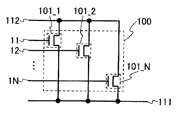
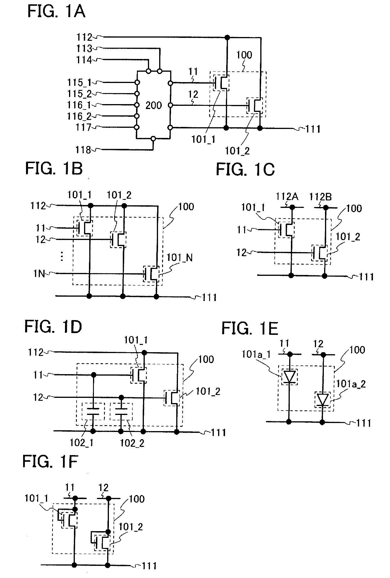
[0119]First, a circuit structure of the semiconductor device in this embodiment is described with reference to FIG. 1A. The semiconductor device shown in FIG. 1A includes a circuit 100 (also referred to as a second control circuit) and a circuit 200 (also referred to as a first control circuit). The circuit 100 includes a plurality of transistors which are transistors 101_1 and 101_2.

[0120]Note that the transistors 101_1 and 101_2 are n-channel transistors, for example. An n-channel transistor is turned on when a potential difference (Vgs) between a gate and a source is larger than threshold voltage (Vth). Note...

embodiment 2

[0218]In this embodiment, a specific example of the circuit 200 described in Embodiment 1 is described. Note that the circuit 200 can also be referred to as a semiconductor device or a driver circuit. Note that description of the content described in Embodiment 1 is omitted. Note that a content described in this embodiment can be freely combined with the content described in Embodiment 1.

[0219]First, an example of the circuit 200 is described with reference to FIG. 6A. In an example of FIG. 6A, the circuit 200 includes a circuit 300 which shows a part of the circuit 200. The circuit 300 can include one transistor or a plurality of transistors, for example. These transistors preferably have the same polarity as the transistors 101_1 and 101_2. However, this embodiment is not limited thereto.

[0220]The circuit 300 is connected to the wiring 115_1, the wiring 115_2, the node 11, and the node 12. Note that this embodiment is not limited thereto. The circuit 300 can be connected to a vari...

embodiment 3

[0287]In this embodiment, a specific example of the circuit 200 which is different from that in Embodiment 2 is described. Note that description of the content described in Embodiments 1 and 2 is omitted. Note that a content described in this embodiment can be freely combined with the content described in Embodiments 1 and 2.

[0288]First, one example of the circuit 200 is described with reference to FIG. 15A. In one example in FIG. 15A, the circuit 200 includes a circuit 400. For example, the circuit 400 is a part of the circuit 200. The circuit 400 can include one or more transistors. These transistors preferably have the same polarity as the transistors 101_1 and 101_2. However, this embodiment is not limited thereto.

[0289]Note that as shown in FIG. 15B, the circuit 200 can include the circuit 300 described in Embodiment 2 in addition to the circuit 400. Note that a part of or the whole of the circuit 300 can be used as a part of or the whole of the circuit 400. In addition, a part...


PUM


Abstract

It is an object to suppress deterioration in characteristics of a transistor in a driver cricuit. A driver circuit includes a first transistor, a second transistor including a gate and one of a source and a drain to which a second signal is inputted, a third transistor whose gate is electrically connected to one of a source and a drain of the first transistor and which controls whether a voltage state of an output signal is set or not by being turned on/off, and a fourth transistor whose gate is electrically connected to the other of the source and the drain of the second transistor and which controls whether a voltage state of an output signal is set or not by being turned on/off.

Description

BACKGROUND OF THE INVENTION[0001]1. Field of the Invention[0002]The present invention relates to a semiconductor device, a display device, a liquid crystal display device, a light-emitting device, a method for driving these devices, and a method for manufacturing these devices. The present invention particularly relates to a semiconductor device, a display device, a liquid crystal display device, and a light-emitting device which include a driver circuit formed over the same substrate as a pixel portion, and a method for driving these devices. Further, the present invention relates to an electronic device including the semiconductor device, the display device, the liquid crystal display device, and the light emitting device.[0003]2. Description of the Related Art[0004]In recent years, with the increase of large display devices such as liquid crystal televisions, display devices have been actively developed. In particular, a technique for forming a driver circuit such as a gate drive...

Claims


Application Information

Patent Timeline
Patent Type & Authority Applications(United States)
IPC IPC(8): G11C19/28H01L27/085H03K3/289
CPCG09G3/3614G09G3/3677G09G3/3688H03K19/00369G09G2320/043G11C19/28G09G2310/0286
Inventor KIMURA, HAJIMEUMEZAKI, ATSUSHI
Owner SEMICON ENERGY LAB CO LTD
Why Eureka
Try Eureka