Semiconductor device, active matrix substrate, and display device

a technology of active matrix substrate and semiconductor device, applied in non-linear optics, instruments, optics, etc., can solve the problem that etching defects tend to occur in the vicinity of step portions at lower layers of lines, and achieve the effect of suppressing characteristic deteriorations of semiconductor devi

Active Publication Date: 2014-07-15
SHARP KK
View PDF12 Cites 1 Cited by
  • Summary
  • Abstract
  • Description
  • Claims
  • Application Information

AI Technical Summary

Benefits of technology

[0018]According to a semiconductor device disclosed in the present application, the present invention can sufficiently suppress characteristic deteriorations of a semiconductor device due to misalignment.

Problems solved by technology

In a semiconductor device such as TFTs, in the process of forming lines by wet etching, etching defects tend to occur in the vicinity of step portions at lower layers of the lines.

Method used


Image

  • Semiconductor device, active matrix substrate, and display device
  • Semiconductor device, active matrix substrate, and display device
  • Semiconductor device, active matrix substrate, and display device

Examples


embodiment 1

[0035]Hereinafter, preferred embodiments of a semiconductor device, an active matrix substrate and a display device of the present invention will be described with reference to the drawings. In the following description, the present invention is applied to a transmission type liquid crystal display device.

[0036][Configuration Example of Liquid Crystal Display Device]

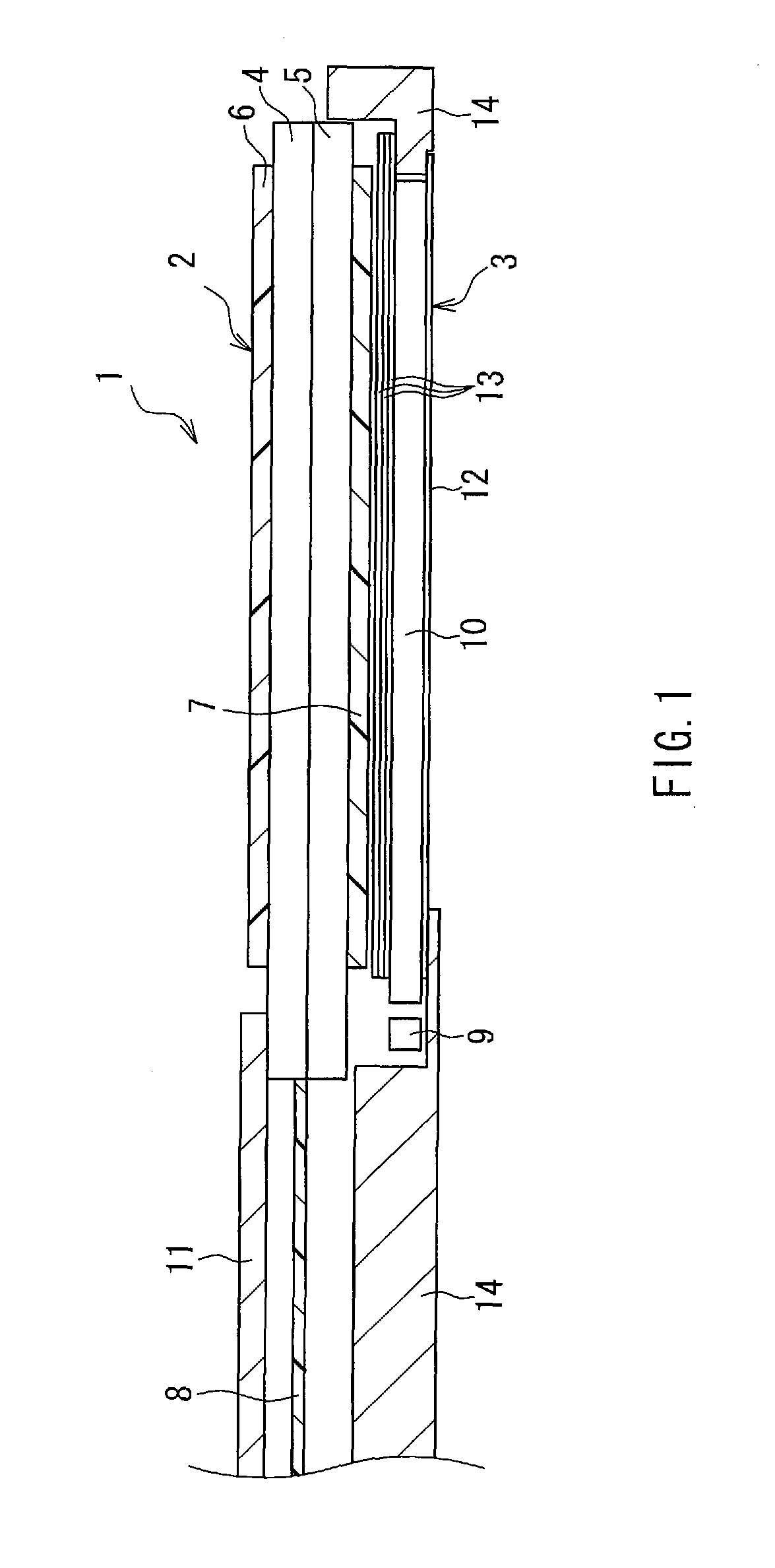
[0037]FIG. 1 is a view illustrating a liquid crystal display device according to one embodiment of the present invention. In FIG. 1, a liquid crystal display device 1 of the present embodiment is provided with a liquid crystal panel 2 and a backlight device 3. An upper side of the liquid crystal panel 2 in FIG. 1 is defined as a viewing side (display surface side). The backlight device 3 is arranged on a non-display surface side (lower side in FIG. 1) of the liquid crystal panel 2 and generates illumination light for illuminating the liquid crystal panel 2.

[0038]The liquid crystal panel 2 includes a color filter substrat...

modified example 1

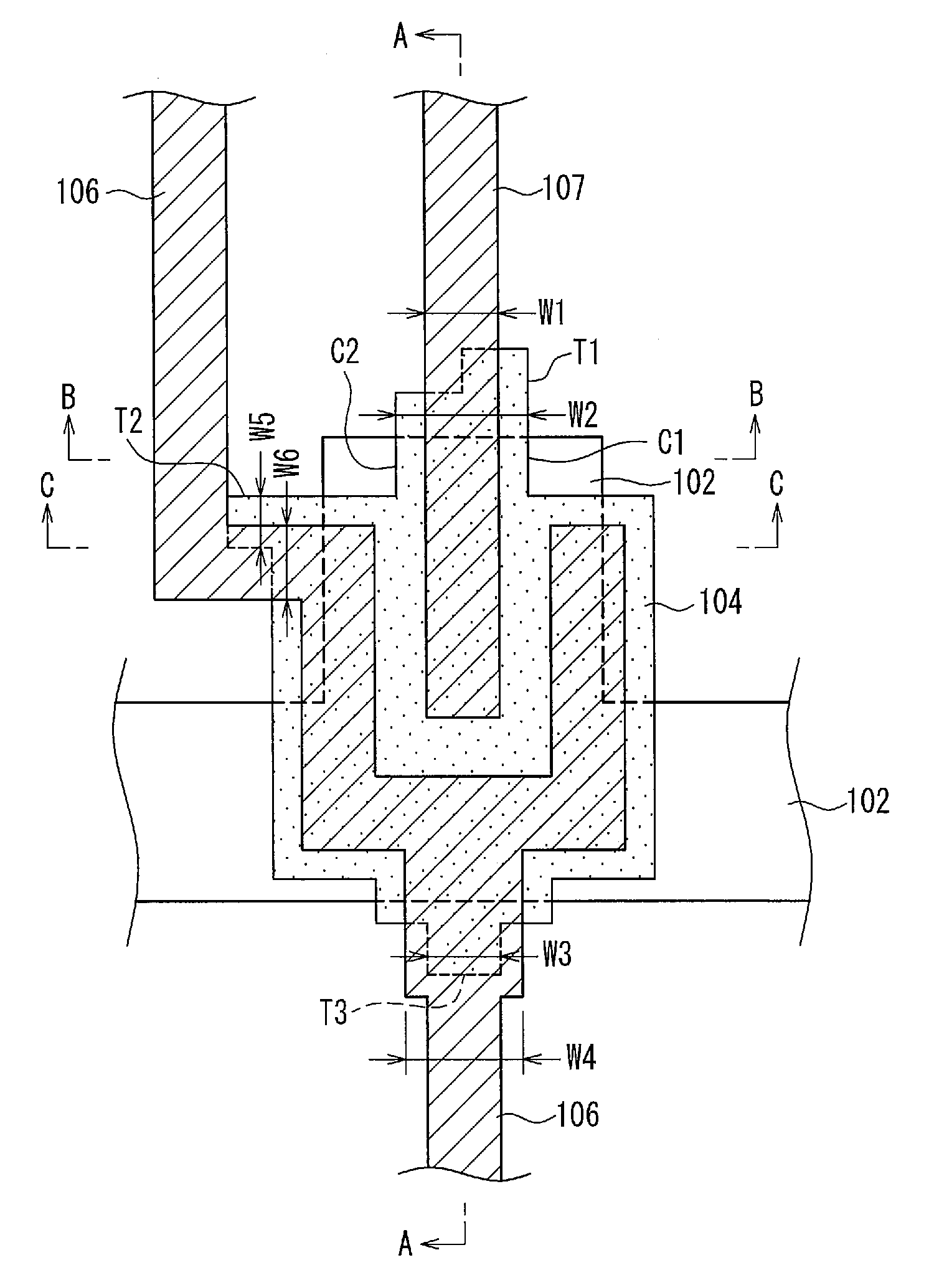
[0084]FIG. 5 is a plan view showing a modification example of the configuration of the thin film transistor 18. In the example shown in FIG. 5, the drain electrode 107 is formed so as to extend parallel to the extending direction of gate lines drawn out from the gate electrode 102. The source electrode 106 is arranged so as to surround both sides and a tip of the drain electrode 107 extending linearly. The channel region of the semiconductor layer 104 is formed under the region sandwiched between the drain electrode 107 and the source electrode 106 surrounding the drain electrode 107. Two source lines extending in a direction perpendicular to the extending direction of the gate lines are connected to the source electrode 106.

[0085]Further, the semiconductor layer 104 has a portion that protrudes in the extending direction of the drain electrode 107. In the tip of the protruding portion, the semiconductor layer 104 has, at a portion overlapping the drain electrode 107, the protrusion...

embodiment 2

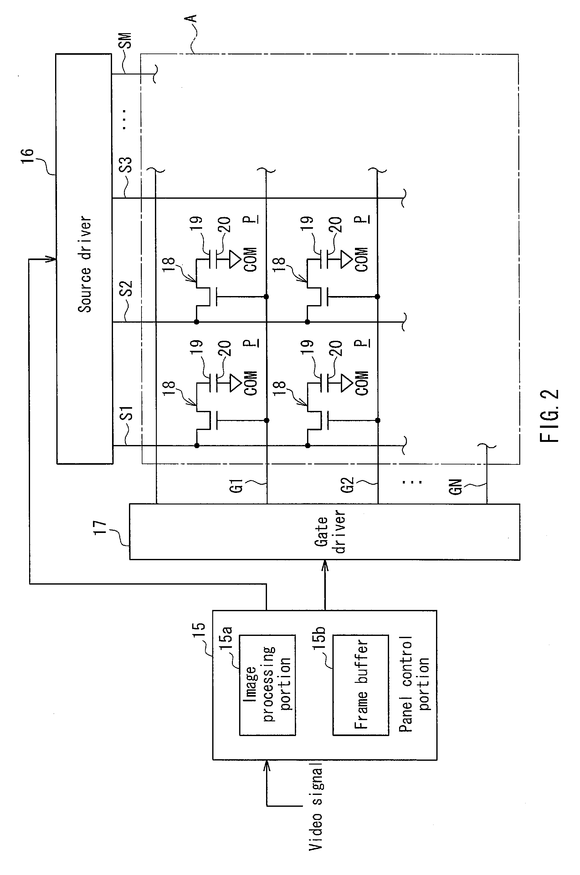
[0115]FIG. 12 is a plan view showing a configuration example of thin film transistors according to Embodiment 2. FIG. 12 shows a configuration example of two thin film transistors 18 adjacent to each other on the active matrix substrate 5 and a configuration example of the peripheral lines. Each of the thin film transistors 18 includes the gate electrode 102, the semiconductor layer 104 formed on the gate electrode 102, the source electrode 106 formed in a comb shape, and two drain electrodes 107c, 107d opposed to each other with the source electrode 106 and the channel region interposed therebetween. Drain lines are drawn out respectively from the drain electrodes 107c, 107d so as to be connected to pixel electrodes (not shown). As described above, by forming the source electrode 106 and the plurality of the drain electrodes 107c, 107d corresponding to the source electrode 106 on the gate electrode 102 and the semiconductor layer 104 and drawing out the drain lines from the respect...


PUM

PropertyMeasurementUnit
thicknessaaaaaaaaaa
thicknessaaaaaaaaaa
thicknessaaaaaaaaaa

Abstract

A semiconductor device (18) includes: a gate electrode (102) formed on a substrate (101); a semiconductor layer (104) formed above the gate electrode (102) and including a source region, a drain region, and a channel region; a source electrode (106) connected to the source region above the semiconductor layer (104); and a drain electrode (107) connected to the drain region above the semiconductor layer (104). The semiconductor layer (104) has, at a portion overlapping the drain electrode (107), a protrusion that protrudes outward along an extending direction of a drain line drawn out from the drain electrode (107). At an outside of the channel region sandwiched between the drain electrode (107) and the source electrode (106), the semiconductor layer (104) has an adjustment portion where an outer boundary of the semiconductor layer (104) is positioned more inward than an outer boundary of the gate electrode (102).

Description

TECHNICAL FIELD[0001]The present invention relates to a semiconductor device provided with a transistor, and an active matrix substrate and a display device using the semiconductor device.BACKGROUND ART[0002]TFTs are formed on an active matrix substrate of a liquid crystal display device. In a semiconductor device such as TFTs, in the process of forming lines by wet etching, etching defects tend to occur in the vicinity of step portions at lower layers of the lines. Because of this, in the process of producing the liquid crystal display device, for example, a line resistance is increased due to disconnection or partial disconnection of the lines, which sometimes decreases productivity and display quality. To deal with this, a line configuration has been proposed for suppressing the line width from being narrow in the step portion and the line from being disconnected (e.g., see Patent Document 1). Further, a configuration has been proposed that prevents disconnection of a drain line ...

Claims


Application Information

Patent Timeline
Patent Type & Authority Patents(United States)
IPC IPC(8): H01L29/04H01L29/417G02F1/1362H01L31/036H01L29/10H01L29/786G02F1/1368H01L31/00H01L29/15H01L29/423
CPCG02F2001/13629H01L29/42384H01L29/41733H01L29/78696G02F1/136286G02F1/1368G02F1/13629
Inventor OKAZAKI, SHOJIYANEDA, TAKESHINAKAMURA, WATARUKATSUI, HIROMITSU
Owner SHARP KK
Why Eureka
Try Eureka