Off-axis pinned layer magnetic element utilizing spin transfer and an MRAM device using the magnetic element

a magnetic element and spin transfer technology, applied in the field of magnetic memory systems, can solve the problems of increasing the area and complexity of b>20/b>, limiting the write current amplitude, and increasing the cross talk and power consumption, so as to achieve a high output signal and a magnetic memory, and shorten the write time

Inactive Publication Date: 2005-05-03
SAMSUNG SEMICON
View PDF1 Cites 308 Cited by
  • Summary
  • Abstract
  • Description
  • Claims
  • Application Information

AI Technical Summary

Benefits of technology

[0013]The present invention provides a method and system for providing a magnetic element capable of being written using the spin-transfer effect while generating a high output signal and a magnetic memory using the magnetic element. The magnetic element comprises a first ferromagnetic pinned layer, a nonmagnetic intermediate layer, and a ferromagnetic free layer. The first pinned layer has a first magnetization pinned in a first direction. The nonmagnetic intermediate layer resides between the first pinned layer and the free layer. The free layer has a second magnetization with an easy axis in a second direction. The first direction is in the same plane as the second direction and is oriented at an angle with respect to the second direction. This angle is different from zero and π radians. The magnetic element is also configured to allow the second magnetization of the free layer to change direction due to spin transfer when a write current is passed through the magnetic element.
[0014]According to the system and method disclosed herein, the present invention provides a magnetic element and a magnetic memory that is capable of being written using the more efficient and localized spin-transfer mechanism while allowing for a shorter write time.

Problems solved by technology

This large current can cause a host of problems in the conventional magnetic niemory 10.
For example, cross talk and power consumption would increase.
In addition, the driving circuits required to drive the current that generates the switching field at the desired memory cell 20 would also increase in area and complexity.
This upper limit on the write current amplitude can lead to reliability issues because the cells that are harder to switch than others (due to fabrication and material nonuniformity) will fail to write consistently.

Method used


Image

  • Off-axis pinned layer magnetic element utilizing spin transfer and an MRAM device using the magnetic element
  • Off-axis pinned layer magnetic element utilizing spin transfer and an MRAM device using the magnetic element
  • Off-axis pinned layer magnetic element utilizing spin transfer and an MRAM device using the magnetic element

Examples


first embodiment

[0073]FIGS. 8A-8C are more detailed embodiments of various methods for performing the process 200. FIG. 8A is a flow chart depicting a method 200′ in accordance with the present invention for providing a magnetic element in accordance with the present invention. For clarity, the method 200′ is described in the context of the magnetic element 100. However, the method 200′ could be adapted to other magnetic elements. The antiferromagnetic layer 102 is provided, via step 202′. In a preferred embodiment, the antiferromagnetic layer 102 is provided on the appropriate seed layer. The pinned layer 104 is provided in step 204′. Step 204′ could include providing a synthetic pinned layer. The nonmagnetic intermediate layer 106 is provided in step 206′. The free layer 108 having an easy axis in a particular direction is provided in step 208′. Step 208′ could include providing a synthetic free layer. The antiferromagnetic layer 102 is annealed at the appropriate temperature and field in order t...

second embodiment

[0074]FIG. 8B is a flow chart depicting a method 200″ in accordance with the present invention for providing a magnetic element in accordance with the present invention. For clarity, the method 200″ is described in the context of the magnetic element 100. However, the method 200″ could be adapted to other magnetic elements. The antiferromagnetic layer 102 may optionally be provided, via step 202″. In a preferred embodiment, the antiferromagnetic layer 102 is provided on the appropriate seed layer. Flowever, the antiferromagnetic layer 102 may be omitted, in favor of, for example, using just high coercivity induced by shape anisotropy and / or. crystalline anisotropy. The pinned layer 104 is provided in step 204″. Step 204″ could include providing a synthetic pinned layer. The nonmagnetic intermediate layer 106 is provided in step 206″. The free layer 108 having an easy axis in a particular direction is provided in step 208″. Step 208″ could include providing a synthetic free layer. Th...

third embodiment

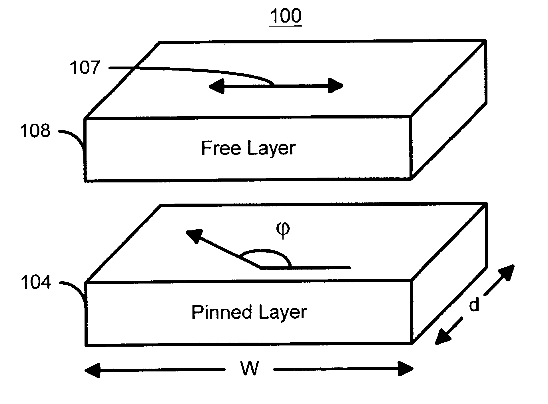
[0075]FIG. 8C is a flow chart depicting a method in accordance with the present invention for providing a magnetic element in accordance with the present invention. For clarity, the method 200′″ is described in the context of the magnetic element 100. However, the method 200′″ could be adapted to other magnetic elements. The pinned layer 104 having a low magnetic anisotropy is provided in step 204′″. Step 204′″ could include providing a synthetic pinned layer. The nonmagnetic intermediate layer 106 is provided in step 206′″. The free layer 108 having an easy axis in a particular direction is provided in step 208′″. The free layer 108 provided in step 208′″ has a higher anisotropy than the pinned layer 104. Step 208′″ could include providing a synthetic free layer. An external magnetic field is applied to ensure that the magnetization of the pinned layer 104 is oriented at an angle, φ, with respect to the direction in which easy axis 107 of the free layer 108 is set, via step 211.

[00...


PUM


Abstract

A method and system for providing a magnetic element capable of being written in a reduced time using the spin-transfer effect while generating a high output signal and a magnetic memory using the magnetic element are disclosed. The magnetic element includes a ferromagnetic pinned layer, a nonmagnetic intermediate layer, and a ferromagnetic free layer. The pinned layer has a magnetization pinned in a first direction. The nonmagnetic intermediate layer resides between the pinned layer and the free layer. The free layer has a magnetization with an easy axis in a second direction. The first direction is in the same plane as the second direction and is oriented at an angle with respect to the second direction. This angle is different from zero and π radians. The magnetic element is also configured to allow the magnetization of the free layer to change direction due to spin transfer when a write current is passed through the magnetic element.

Description

CROSS-REFERENCE TO RELATED APPLICATIONS[0001]This application is related to U.S. patent application Ser. No. 10 / 213,537, entitled “Magnetic Element Utilizing Spin Transfer and an MRAM Device Using the Magnetic Element,” filed Aug. 6, 2002, and assigned to the Assignee of the present application.FIELD OF THE INVENTION[0002]The present invention relates to magnetic memory systems, and more particularly to a method and system for providing an element that employs a spin transfer effect in switching, that requires a lower current for switching, and that can be used in a magnetic memory such as magnetic random access memory (“MRAM”).BACKGROUND OF THE INVENTION[0003]Magnetic memories are often used in storing data. One type of memory element currently of interest utilizes magnetoresistance of a magnetic element for storing data. FIGS. 1A and 1B depict conventional magnetic elements 1 and 1′. The conventional magnetic element 1 is a spin valve 1 and includes a conventional antiferromagneti...

Claims


Application Information

Patent Timeline
Patent Type & Authority Patents(United States)
IPC IPC(8): G11C11/15G11C11/02
CPCG11C11/15
Inventor NGUYEN, PAUL P.HUAI, YIMING
Owner SAMSUNG SEMICON
Why Eureka
Try Eureka