Integrated circuit
a technology of integrated circuits and integrated circuits, applied in the direction of logic circuit coupling/interface arrangements, pulse techniques, instruments, etc., can solve the problems of reducing the withstand voltage of the output mos transistor, affecting the withstand voltage, so as to reduce the circuit area of the output transistor and the chip area, the effect of reducing the circuit area
- Summary
- Abstract
- Description
- Claims
- Application Information
AI Technical Summary
Benefits of technology
Problems solved by technology
Method used
Image
Examples
first embodiment
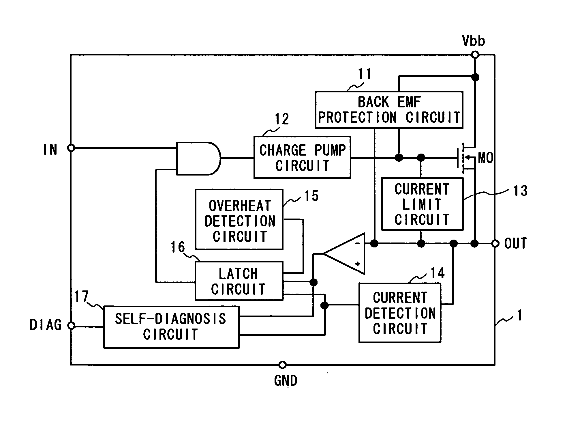
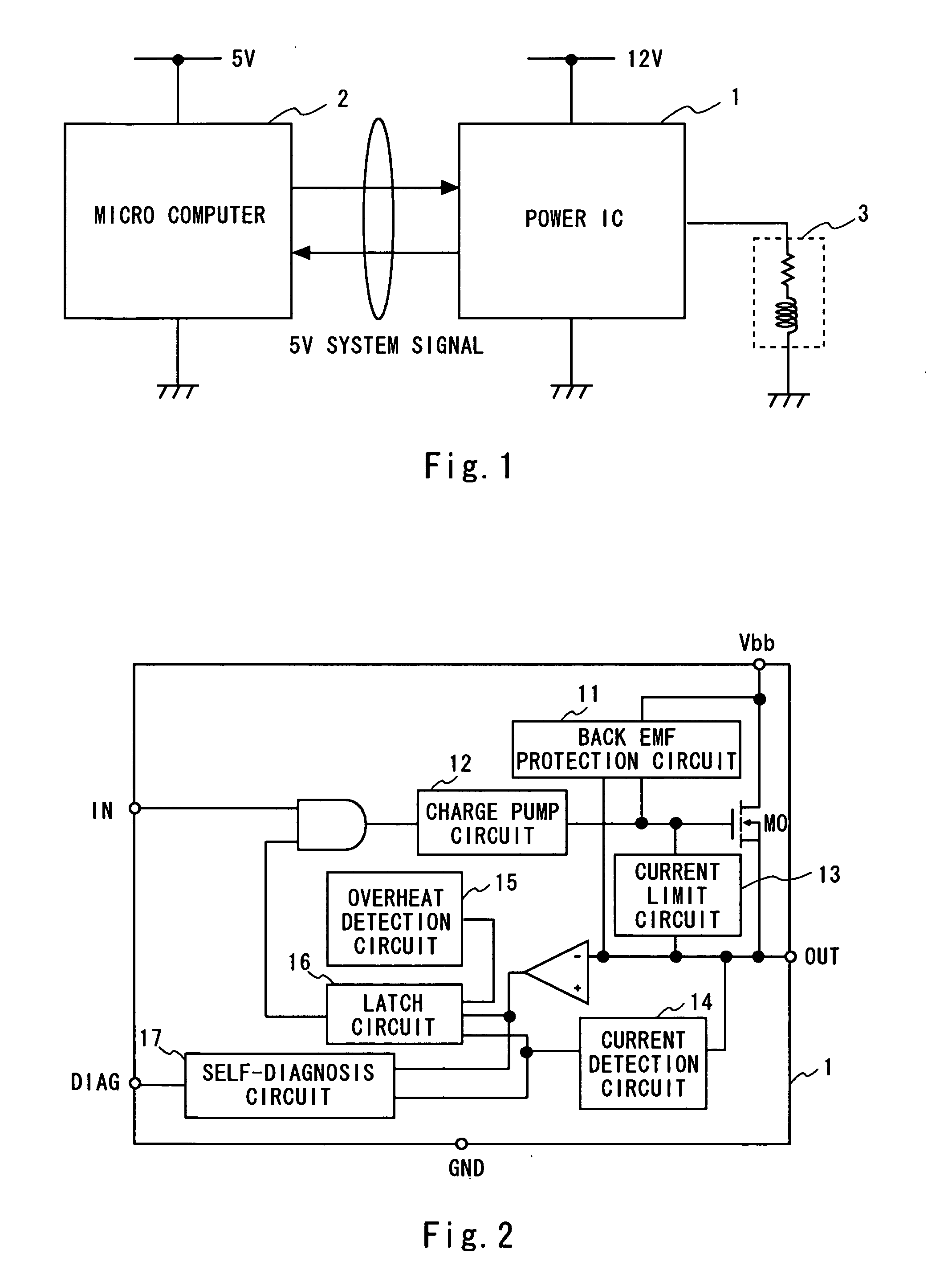
[0043] Referring first to FIG. 1, the configuration of a system having a power IC according to a first embodiment of the invention is explained. The system controls the current flowing into an L load. It includes a power IC 1, a microcomputer 2, and an L load 3. Though the power IC 1 and the microcomputer 2 are each an integrated circuit on one chip in this example, they may be implemented on a given number of chips.
[0044] The microcomputer 2 is connected to the power IC 1 to exchange signals. The microcomputer 2 transmits to the power IC 1 a control signal which controls the current of the L load 3 and receives from the power IC 1 a diagnostic signal which indicates the state of the power IC 1 and so on. The microcomputer 2 is, for example, driven by a power source of 5V, and the signal transmitting to or receiving from the power IC 1 has an amplitude of 5V.
[0045] The power IC 1 is connected to the microcomputer 2 and to the L load 3. The power IC 1 controls the current flowing i...
second embodiment
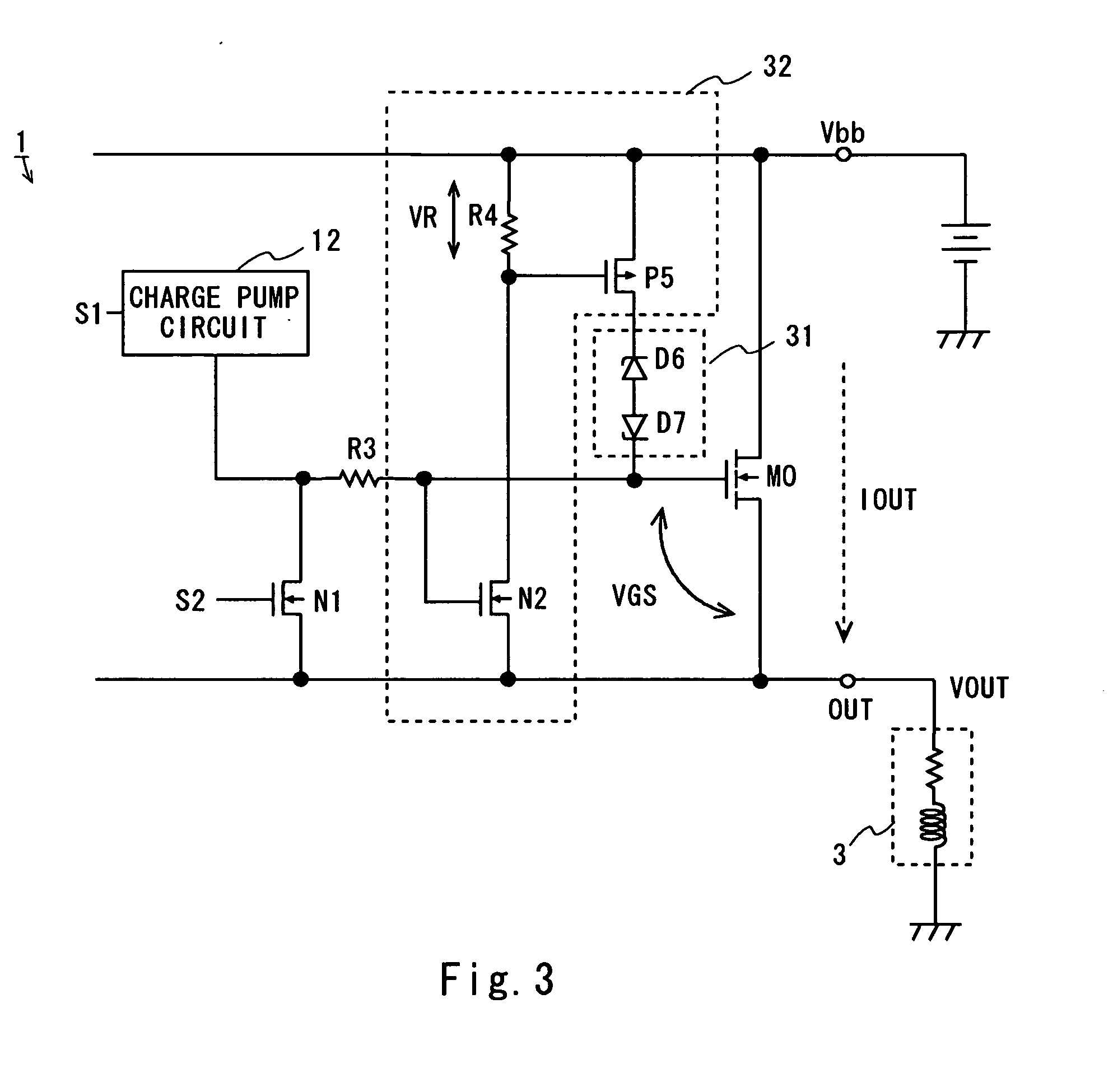
[0077] Referring now to FIG. 6, the circuit configuration of a power IC of a second embodiment is explained. Like FIG. 3, FIG. 6 illustrates the part of the circuit including the output MOS transistor M0, the back EMF protection circuit 11, and the charge pump circuit 12 of the power IC 1 of FIG. 2.
[0078] The power IC 1 of this embodiment has a resistor R3′ between the resistor R3 and the gate of the output MOS transistor MO in addition to the elements shown in FIG. 3. The gate of the gate detection MOS transistor N2 is connected to a node between the resistor R3 and the resistor R3′.
[0079] In this embodiment, the gate detection MOS transistor N2 refers to the gate voltage of the output MOS transistor M0 which drops across the resistor R3′. This configuration also allows the same operation as the configuration of FIG. 3.
third embodiment
[0080] Referring then to FIG. 7, the circuit configuration of a power IC of a third embodiment is explained. Like FIG. 3, FIG. 7 illustrates the part of the circuit including the output MOS transistor M0, the back EMF protection circuit 11, and the charge pump circuit 12 of the power IC 1 of FIG. 2.
[0081] The power IC 1 of this embodiment has a constant current source I1 and a diode D8 between the Vbb terminal and the gate of the output MOS transistor M0 in addition to the elements shown in FIG. 3. The gate of the gate detection MOS transistor N2 is connected to a node between the constant current source I1 and the diode D8.
[0082] In this embodiment, the gate detection MOS transistor N2 refers to the gate voltage of the output MOS transistor M0 which is boosted by the diode D8. This configuration also allows the same operation as the configuration of FIG. 3.
PUM
 Abstract
Description
Claims
Application Information


