Scan driver and display device including the same

a display device and scan driver technology, applied in the field of scan driver and display device, can solve the problems of comparatively higher cost than the pmoled display, difficult to realize the control method, and difficulty in large size or high accuracy of the pmoled display, so as to reduce the dead space, reduce the number of circuit elements, and reduce the circuit area of the scan driver

Inactive Publication Date: 2014-04-24
SAMSUNG DISPLAY CO LTD
View PDF11 Cites 34 Cited by
  • Summary
  • Abstract
  • Description
  • Claims
  • Application Information

AI Technical Summary

Benefits of technology

[0010]An exemplary embodiment of the present invention provides for an ultra-light display device using thin film technology by reducing a circuit area of a scan driver and dead space that cannot be used. Another exemplary embodiment of the present invention increases a production yield of the display device by reducing a number of circuit elements to reduce the circuit area of the scan driver.
[0040]According to the above and other embodiments of the present invention, a circuit area of the scan driver may be reduced, thereby reducing a number of circuit elements forming the scan driver, and furthermore reducing dead space that cannot be used in a high-resolution display device. In addition, the layout space of the display device may be relatively increased by a reduction of the circuit area occupied by the scan driver such that design freedom may be increased. Further, the production yield of the display device may be improved by a reduction of the number of the circuit elements of the scan driver.

Problems solved by technology

However, it is difficult to realize a PMOLED panel of a large size or high accuracy.
However, it is difficult to technically realize the control method of the AMOLED display, which results in a comparatively higher cost than the PMOLED display.
In general, the scan driver has a complicated circuit structure to sequentially transmit correct scan signals to the pixels included in the display panel for each pixel line such that an area occupied by the scan driver is large in comparison to the other driving circuits.
In addition, when manufacturing a high resolution display device integrating a large number of pixels for the same panel size, space that cannot be used by other circuits (such as dead space) is increased by a circuit area that is occupied by the scan driver such that it is difficult to manufacture the display device to be ultra-light and as a thin film display device.

Method used


Image

  • Scan driver and display device including the same
  • Scan driver and display device including the same
  • Scan driver and display device including the same

Examples


Embodiment Construction

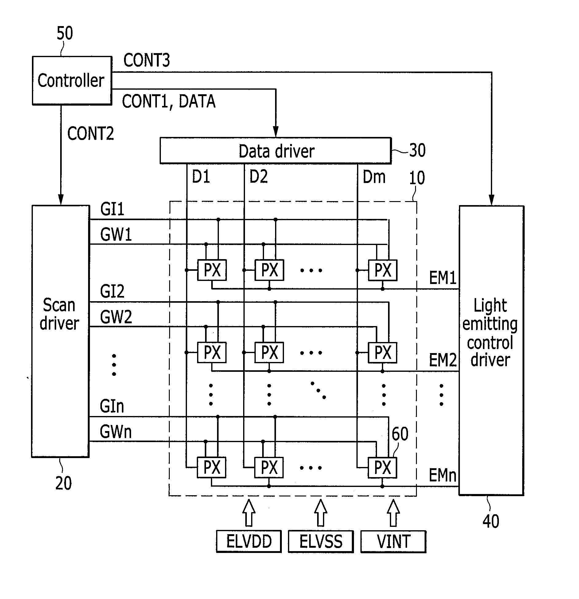
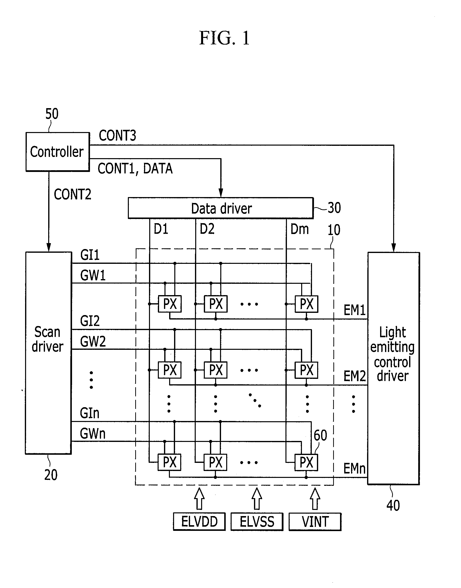
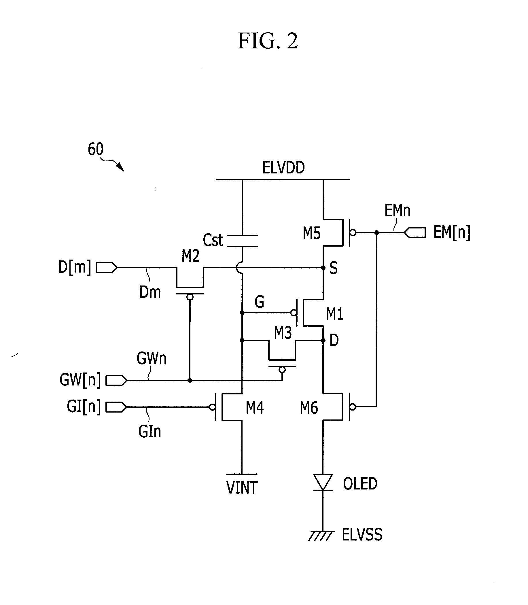
[0049]Hereinafter, the present invention will be described more fully with reference to the accompanying drawings, in which exemplary embodiments of the invention are shown. As those skilled in the art would realize, the described exemplary embodiments may be modified in various different ways, all without departing from the spirit or scope of the present invention. Constituent elements having the same structures throughout the embodiments are denoted by the same reference numerals and are described in a first embodiment. In the other embodiments, only constituent elements other than the same constituent elements are described.

[0050]Throughout this specification and the claims that follow, when it is described that an element is “coupled” to another element, the element may be directly coupled (for example, connected) to the other element or indirectly coupled (for example, electrically connected) to the other element through one or more third other elements. In addition, unless exp...


PUM


Abstract

A scan driver and a display device including the scan driver are provided. The scan driver is configured to drive a plurality of pixels with a plurality of gate signals and includes a plurality of stages, each of the stages including one or more regions, each of the regions including: a plurality of sub-drivers configured to generate ones of the gate signals and to transmit the ones of the gate signals to ones of the pixels; and a driver commonly coupled to the sub-drivers and configured to concurrently supply a common signal to each of the sub-drivers, the driver of one of the one or more regions being configured to receive the common signal of one of the one or more regions of a previous one of the stages during forward direction driving or of a next one of the stages during reverse direction driving.

Description

CROSS-REFERENCE TO RELATED APPLICATION[0001]This application claims priority to and the benefit of Korean Patent Application No. 10-2012-0118557, filed in the Korean Intellectual Property Office on Oct. 24, 2012, the entire content of which is incorporated herein by reference.BACKGROUND[0002](a) Field[0003]Aspects of embodiments of the present invention relate to a scan driver and a display device including the scan driver.[0004](b) Description of the Related Art[0005]Among flat panel displays, the organic light emitting diode (OLED) display, which displays images by using OLEDs that generate light by recombining electrons and holes, has a fast response speed, low power consumption, and excellent emission efficiency, luminance, and viewing angle, such that usage thereof has recently been expanded. Generally, the OLED display is classified as a passive matrix OLED (PMOLED) or an active matrix OLED (AMOLED) according to a driving method of the OLEDs.[0006]The PMOLED uses a method in w...

Claims


Application Information

Patent Timeline
Patent Type & Authority Applications(United States)
IPC IPC(8): G09G3/20
CPCG09G3/20G09G3/3266G09G2310/0286G11C19/28G09G3/30
Inventor LEE, JAE-SICLEE, HYUN
Owner SAMSUNG DISPLAY CO LTD
Why Eureka
Try Eureka