Semiconductor integrated circuit for wireless communication

Inactive Publication Date: 2006-01-19
RENESAS ELECTRONICS CORP
View PDF4 Cites 30 Cited by
  • Summary
  • Abstract
  • Description
  • Claims
  • Application Information

AI Technical Summary

Benefits of technology

[0023] Advantageous effects obtained by typical ones of the inventions disclosed in the present application will be explained in brief as follows:
[0024] According to the present invention, it is not necessary to measure oscillation frequencies in all frequency bands in advance and store them in a memory. Therefore, the time taken until a used frequency band is decided, becomes short and the occupied area of a circuit can be reduced. Since there is provided a delay compensating circuit which applies a delay to a signal divided by a variable divider, it is possible to avoid that a frequency

Problems solved by technology

This is because when an attempt is made to bring a capacitive element having a capacitance value necessary to obtain a desired characteristic into on-chip form, the area of the element becomes very large.
However, thermal noise of the resistive element increases with the increase in resistance value.
The PLL is accompanied by a problem that since the voltage of the loop filter is directly applied to a control terminal of the VCO, the thermal noise produced in the resistive element appears on the output of the VCO when the thermal noise of the resistive element constituting the loop filter is high and the control sensitivit

Method used


Image

  • Semiconductor integrated circuit for wireless communication
  • Semiconductor integrated circuit for wireless communication
  • Semiconductor integrated circuit for wireless communication

Examples


first embodiment

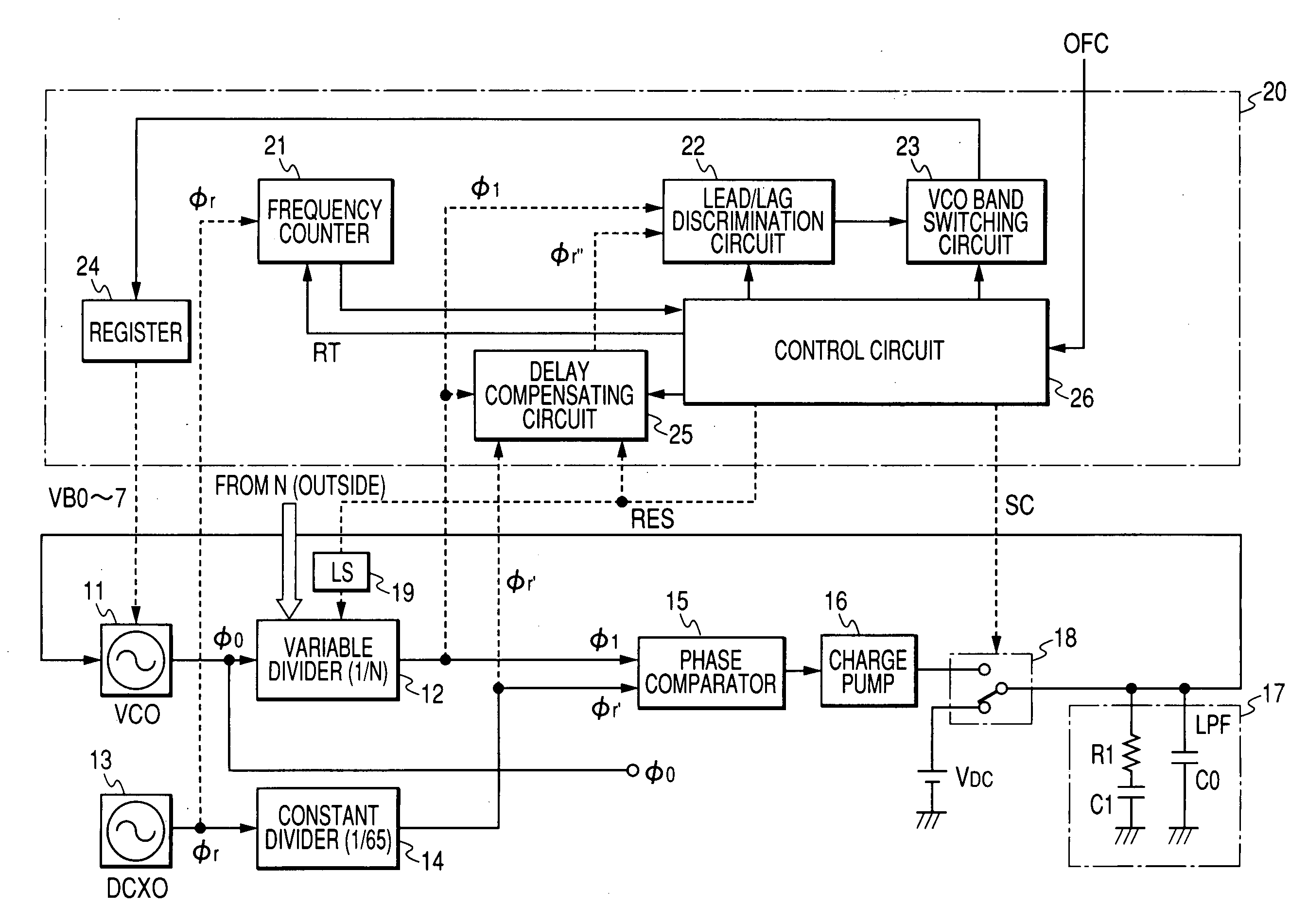
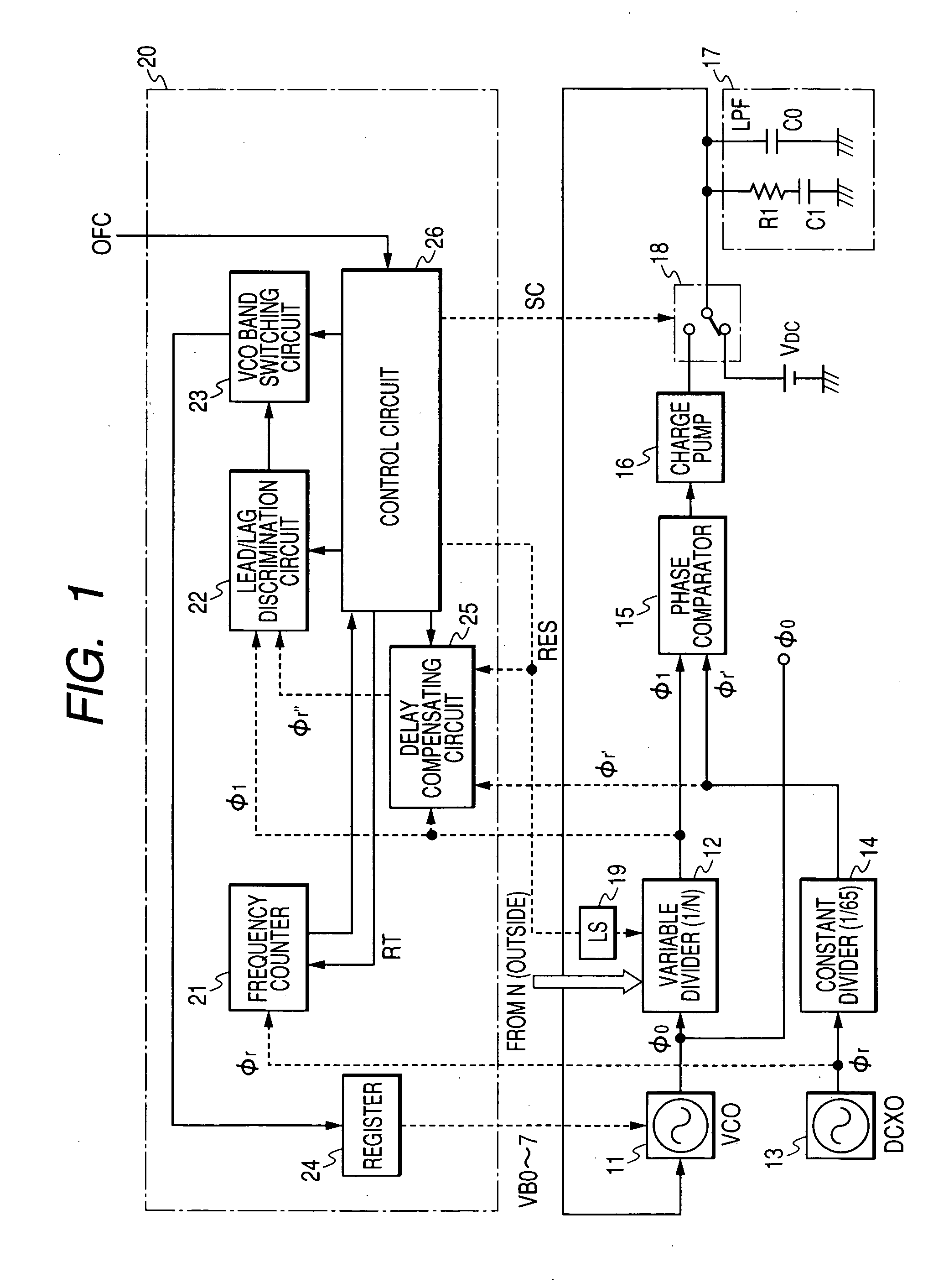
[0068] the delay compensating circuit 25 is shown in FIG. 7. Prior to the description of the configuration and operation of the delay compensating circuit 25 shown in FIG. 7, the reason why the delay compensating circuit 25 is provided, will be explained using a timing chart shown in FIG. 6.

[0069] In the auto band selection circuit employed in the embodiment, in which the phase lead / lag discrimination circuit 22 determines whether the rising edge of the output pulse φ1 of the variable divider 12 leads the rising edge of the output pulse φr′ of the constant divider 14, the rising edge of the output pulse φr′ of the constant divider 14 and the rising edge of the output pulse φ1 of the variable divider 12 coincide with each other upon resetting by the reset signal RES as shown in FIG. 6(A) where no delay occurs in the reset operation of the variable divider 12. It is therefore possible to accurately determine whether the phase processed after 2.5 μs leads or lag.

[0070] On the other ha...

second embodiment

[0079] a delay compensating circuit 25 is shown in FIG. 9. In FIG. 9, the same circuits as those in the delay compensating circuit 25 shown in FIG. 7 are given the same reference numerals and their dual explanations are therefore omitted.

[0080] The delay compensating circuit 25 shown in FIG. 9 is configured in such a manner that a signal φ1 divided by a variable divider 12 and a signal / φr obtained by inverting a pre-division oscillation signal φr of a DCXO 13 by an inverter 27 are selectively inputtable to a signal delay circuit 251 by a switch 252 in place of the reset signal RES and the signal φr′ divided by the constant divider 14, respectively. The delay compensating circuit 25 is provided with a selector switch 256 for selecting either the oscillation signal φr outputted from the DCXO 13 or a signal / φr′ delayed by the signal delay circuit 251 and supplying it to an auto band selection circuit 20. The auto band selection circuit 20 is configured so as to generate a reset signa...


PUM


Abstract

A semiconductor integrated circuit with a PLL (Phase Locked Loop) built therein is used in a semiconductor integrated circuit for wireless communication. The PLL circuit generates an oscillation signal having a predetermined frequency, which is combined with a receive signal or a transmit signal for wireless communication. The PLL circuit includes a VCO capable of switching an oscillation frequency band, a variable divider, a loop filter and a phase comparator. An oscillation frequency of the VCO is controlled according to the difference in phase between a signal obtained by dividing the output of the VCO and a reference signal, and a discrimination circuit makes a decision as to a lead or delay of the phase of an output of the variable divider with respect to a reference signal having a predetermined frequency. An auto band selection circuit generates a signal for selecting a frequency band for the VCO.

Description

CROSS-REFERENCE TO RELATED APPLICATION [0001] The present application claims priority from Japanese patent application No. 2004-210289 filed on Jul. 16, 2004, the content of which is hereby incorporated by reference into this application. BACKGROUND OF THE INVENTION [0002] The present invention relates to a technique effective if applied to a semiconductor integrated circuit with a PLL (Phase Locked Loop) built therein, and relates to, for example, a technique effective if used in a semiconductor integrated circuit for wireless communication, which incorporates therein a PLL circuit that generates an oscillation signal having a predetermined frequency, which is combined with a receive signal or a transmit signal for wireless communication. [0003] In a wireless communication system like a cellular phone, a high-frequency semiconductor integrated circuit (hereinafter called “high-frequency IC”) has been used which includes a PLL circuit including an oscillator that generates a local o...

Claims


Application Information

Patent Timeline
IPC IPC(8): H04B7/00
CPCH03J1/005H03J2200/10H03L7/087H03L7/199H03L7/10H03L7/193H03L7/099H03L7/101
Inventor YAMAMOTO, SATORUOKADA, KAZUHISA
Owner RENESAS ELECTRONICS CORP
Why Eureka
Try Eureka