
Microcrystalline organic semiconductor film, organic semiconductor transistor, and method for producing organic semiconductor transistor

一种有机半导体膜、微晶的技术,应用在半导体/固态器件制造、晶体管、半导体器件等方向,能够解决载流子迁移率降低、有机半导体晶体管性能偏差、晶体结构龟裂等问题

Active Publication Date: 2019-05-21
FUJIFILM CORP
View PDF16 Cites 1 Cited by
  • Summary
  • Abstract
  • Description
  • Claims
  • Application Information

AI Technical Summary

Problems solved by technology

That is, in the techniques described in Patent Documents 1 and 2, if a heating process (firing, sealing process, etc.) Cracks, which cause the carrier mobility to decrease
That is, if the compounds described in the above patent documents are used in the organic semiconductor layer of the transistor, even if the organic semiconductor layer is exposed to heat, variations in the performance of the obtained organic semiconductor transistor are likely to occur.
[0011] In addition, in the technologies described in Patent Documents 1 and 2, the crystal domains of the organic semiconductor layer are relatively large, so the solvent remaining on the lower side of the organic semiconductor layer does not volatilize but tends to remain in the formation process of the organic semiconductor layer.
It is considered that in a bottom-gate transistor, a solvent remains between the gate insulating layer and the organic semiconductor layer, and the residual solvent increases the absolute value of the threshold voltage or becomes a cause of worsening the hysteresis of the threshold voltage.
[0012] In addition, in bottom-contact transistors, the wettability usually differs between the insulating film and the electrodes. Therefore, even when the compounds described in the above-mentioned patent documents are used, it may be difficult to form a layer so large that it covers the entire trench. crystal film
That is, it is sometimes difficult to make the entire organic semiconductor film into a uniform crystalline state, and this is considered to be one of the causes of variation in the performance of the obtained organic semiconductor transistor.

Method used

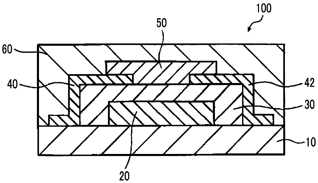
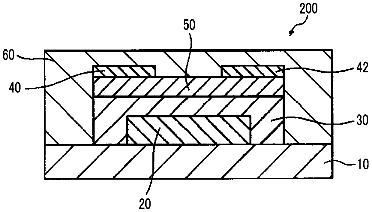
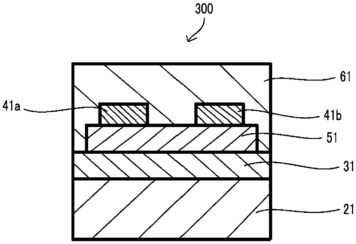

Image

  • Microcrystalline organic semiconductor film, organic semiconductor transistor, and method for producing organic semiconductor transistor
  • Microcrystalline organic semiconductor film, organic semiconductor transistor, and method for producing organic semiconductor transistor
  • Microcrystalline organic semiconductor film, organic semiconductor transistor, and method for producing organic semiconductor transistor

Examples


Embodiment

[0373] Although the present invention will be described in further detail based on examples, the present invention is not limited to the following examples.

Synthetic example 1

[0374] [Synthesis Example 1] Synthesis of Compound 1

[0375] In the following reaction diagram, Bu represents butyl, Et represents ethyl, THF represents tetrahydrofuran, DMF represents N,N-dimethylformamide, TMP represents tetramethylpiperidine, dppf represents 1,1'-bis( Diphenylphosphino)ferrocene.

[0376] -Synthesis of Intermediate 1a-

[0377] [chemical formula 8]

[0378]

[0379] 2,3-Dibromothiophene n-butyl lithium solution (15.9 g, 65.8 mmol) was dissolved in 120 ml of diethyl ether, and n-butyl lithium (1.6 M solution) was added dropwise to the solution while stirring at -90°C. After 30 minutes, a solution obtained by dissolving 2,5-selenophenedicarboxyaldehyde (6.00 g, 32.1 mmol) in 50 ml of tetrahydrofuran was added dropwise, stirred at -78° C. for 20 minutes, and then heated to room temperature. The reaction liquid was quenched with water, and the organic layer was extracted with diethyl ether, and dried over magnesium sulfate. After concentrating with an e...

Synthetic example 2~108

[0406] [Synthesis Examples 2-108] Synthesis of Compounds 2-108

[0407] Compounds 2 to 108 shown in the table below were synthesized in the same manner as in Synthesis Example 1 above, referring to the Examples in JP-A-2015-195362.


PUM

PropertyMeasurementUnit
sizeaaaaaaaaaa
roughnessaaaaaaaaaa
coefficient of variationaaaaaaaaaa

Abstract

To provide: an organic semiconductor film which is capable of effectively inhibiting the formation and expansion of cracks, even if patterned or exposed to high heat; an organic semiconductor transistor in which the organic semiconductor film is used; and a method for producing the organic semiconductor transistor. Provided are: a microcrystalline organic semiconductor film including a compound which has a molecular weight of 3000 or lower, and which is represented by general formula (1), the size of crystal domains in said microcrystalline organic semiconductor film being at least 1 nm, but not more than 100 nm; an organic semiconductor transistor in which the organic semiconductor film is used; and a method for producing the organic semiconductor transistor. X, Y, and Z represent specific ring-forming atoms. R1 and R2 each represent hydrogen, an alkyl group, an alkenyl group, an alkynyl group, an aryl group, or a heteroaryl group. R3 and R4 each represent a halogen, an alkyl group, an alkenyl group, an alkynyl group, an aryl group, or a heteroaryl group. m and n are integers in the range of 0-2.

Description

technical field [0001] The invention relates to a microcrystalline organic semiconductor film, an organic semiconductor transistor and a method for manufacturing the organic semiconductor transistor. Background technique [0002] In logic circuits such as liquid crystal displays, organic electroluminescence displays, and other displays, RFID (radio frequency identifier: RF tags), and memories, tiny transistors are accumulated as switching elements. An organic semiconductor transistor (field-effect transistor) using an organic semiconductor compound as a semiconductor layer can be reduced in weight and is also excellent in flexibility. Therefore, it is attracting attention as a next-generation transistor replacing a transistor having a silicon-based semiconductor layer, and research and development are underway. [0003] In improving the performance of organic semiconductor transistors, improvement of carrier mobility is an important factor. By increasing the carrier mobili...

Claims


Application Information

Patent Timeline
Patent Type & Authority Applications(China)
IPC IPC(8): H01L51/40H01L21/336H01L29/786H01L51/05H01L51/30
CPCH01L29/786C07D517/14C07D493/14C07D495/14C07D513/14C07D498/14H10K71/164H10K85/653H10K85/655H10K85/654H10K85/6576H10K85/6574H10K85/657H10K10/484H10K85/6572H10K10/40H10K10/00
Inventor 后藤崇福崎英治渡边哲也
Owner FUJIFILM CORP
Learn More