OLED display substrate and manufacturing method thereof, display panel and display device

A technology for displaying substrates and substrates, which is applied in the direction of semiconductor devices, electrical components, circuits, etc., can solve the problems of FMM production difficulties, evaporation and color mixing, etc., and achieve the effect of improving the display effect and avoiding color mixing

Inactive Publication Date: 2019-05-31
KUNSHAN GO VISIONOX OPTO ELECTRONICS CO LTD
View PDF8 Cites 3 Cited by
  • Summary
  • Abstract
  • Description
  • Claims
  • Application Information

AI Technical Summary

Problems solved by technology

In the existing technology, there are problems of FMM manufacturing difficulty or vapor deposition color mixing, and it is difficult to further improve PPI

Method used


Image

  • OLED display substrate and manufacturing method thereof, display panel and display device
  • OLED display substrate and manufacturing method thereof, display panel and display device
  • OLED display substrate and manufacturing method thereof, display panel and display device

Examples


Embodiment Construction

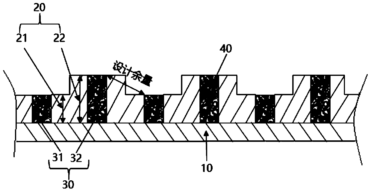
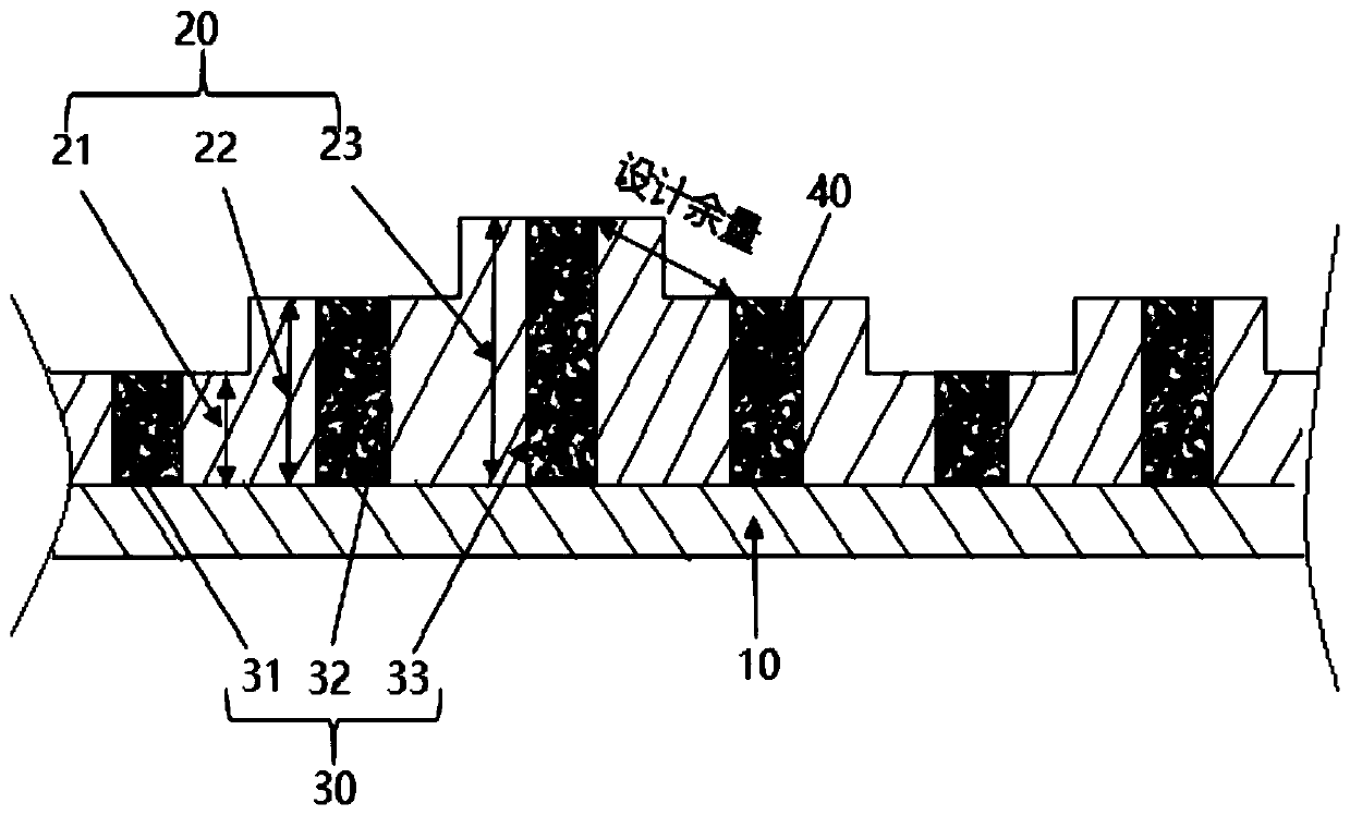
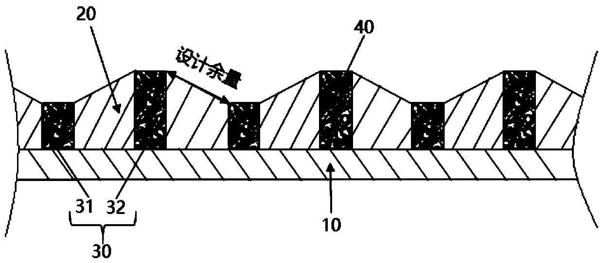
[0034] The characteristics and exemplary embodiments of various aspects of the present invention will be described in detail below. In order to make the purpose, technical solutions and advantages of the present invention more clear, the present invention will be further described in detail below in conjunction with the accompanying drawings and embodiments. It should be understood that the specific embodiments described here are only configured to explain the present invention, not to limit the present invention. It will be apparent to one skilled in the art that the present invention may be practiced without some of these specific details. The following description of the embodiments is only to provide a better understanding of the present invention by showing examples of the present invention.

[0035] It should be noted that in this article, relational terms such as first and second are only used to distinguish one entity or operation from another entity or operation, and ...


PUM


Abstract

The invention discloses an organic light-emitting diode OLED display substrate and a manufacturing method thereof, a display panel and a display device. A substrate and pixel limitation layers arranged on the substrate are included. Each pixel limitation layer has an opening limiting the light emitting area of an organic light emitting component. The pixel limitation layers have at least two thicknesses, and the heights of the openings where the two adjacent organic light emitting components with different colors are located are different. PPI can be increased and the risk of color mixing is avoided.

Description

technical field [0001] The invention relates to the field of display technology, in particular to an organic light emitting diode (OLED) display substrate, a preparation method, a display panel and a display device. Background technique [0002] Organic light-emitting diode (Organic Light-Emitting Diode, OLED) display is recognized by the industry as the successor to liquid crystal due to its many advantages such as thinness, active light emission, fast response, wide viewing angle, rich colors, high brightness, low power consumption, and high and low temperature resistance. The third-generation display technology after the display (Liquid Crystal Display, LCD) can be widely used in terminal products such as smart phones, tablet computers, and televisions. [0003] The number of pixels per inch (Pixel Per Inch, PPI) is getting higher and higher, which has become the development direction of display technology. The higher the PPI, the richer the picture details. There are ma...

Claims


Application Information

Patent Timeline
IPC IPC(8): H01L27/32
Inventor 刘权张露张金方胡思明韩珍珍
Owner KUNSHAN GO VISIONOX OPTO ELECTRONICS CO LTD
Why Eureka
Try Eureka