Cutting method of LED chip with no inclined crack angle, optical lens assembly and laser cutting equipment

A technology of LED chip and cutting method, applied in laser welding equipment, welding equipment, metal processing equipment and other directions, to achieve the effect of satisfying optoelectronic characteristics and improving yield rate

Inactive Publication Date: 2019-06-04
HANS LASER TECH IND GRP CO LTD
View PDF6 Cites 3 Cited by
  • Summary
  • Abstract
  • Description
  • Claims
  • Application Information

AI Technical Summary

Problems solved by technology

[0003] The main purpose of the present invention is to provide a cutting method for LED chips without oblique crack angle, aiming at solving the problem that the oblique crack angle cannot be strictly controlled within 1.5 degrees and the photoelectric characteristics are not damaged during LED chip cutting. technical problem

Method used


Image

  • Cutting method of LED chip with no inclined crack angle, optical lens assembly and laser cutting equipment
  • Cutting method of LED chip with no inclined crack angle, optical lens assembly and laser cutting equipment
  • Cutting method of LED chip with no inclined crack angle, optical lens assembly and laser cutting equipment

Examples


Embodiment Construction

[0021] The technical solutions in the embodiments of the present invention will be clearly and completely described below with reference to the accompanying drawings in the embodiments of the present invention. Obviously, the described embodiments are only a part of the embodiments of the present invention, not all of the embodiments. Based on the embodiments of the present invention, all other embodiments obtained by those of ordinary skill in the art without creative efforts shall fall within the protection scope of the present invention.

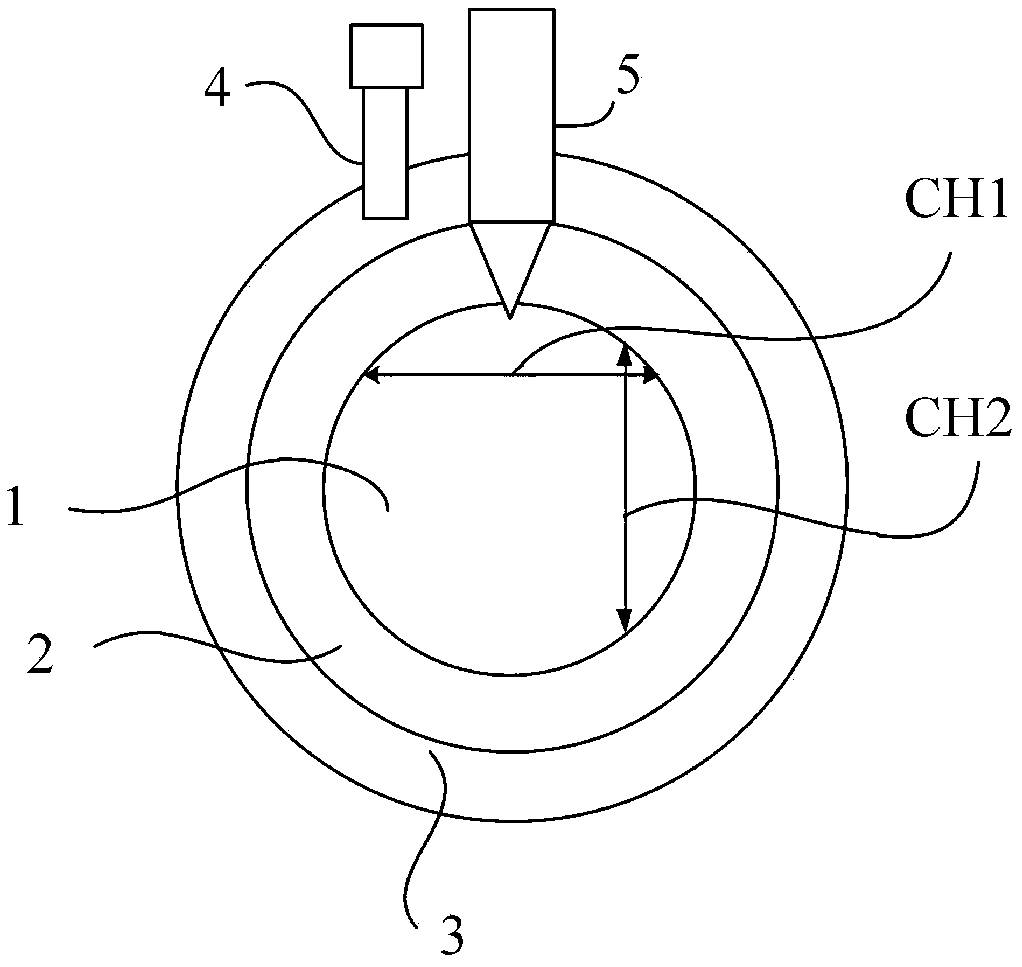
[0022] It should be noted that all directional indications (such as up, down, left, right, front, back, etc.) in the embodiments of the present invention are only used to explain the relationship between various components under a certain posture (as shown in the accompanying drawings). The relative positional relationship, the movement situation, etc., if the specific posture changes, the directional indication also changes accordingly. ...


PUM


Abstract

The invention discloses a cutting method based on an LED chip with no inclined crack angle, an optical lens assembly and laser cutting equipment. According to the cutting method, a wafer taking sapphire as a substrate is cut, and the wafer is located on the front surface of the sapphire. The cutting method comprises the following steps that the spot diameter of laser beams emitted by a laser are increased through a beam expander, and then light spots are compressed into a preset diameter through a first adjustable raster; and the laser beams pass through a laser beam shaping lens assembly andare transformed into Bessel ring-type beams, and the Bessel ring-type beams are focused to the back side of the sapphire for cutting vertically. The laser beams emitted by the laser sequentially passthrough the beam expander, the first adjustable raster and the laser beam shaping lens assembly and then are transformed into reduced Bessel ring beams to cut sapphire wafers. The cutting method realizes that the cut LED chip has no inclined crack angle, and meanwhile, the photoelectric property of the LED chip is guaranteed.

Description

technical field [0001] The invention relates to the technical field of laser processing, in particular to a method for cutting an LED chip without an oblique crack angle, an optical lens assembly and a laser cutting device using the optical lens assembly. Background technique [0002] With the development of science and technology, LED chip cutting technology has been widely studied. In traditional LED chip cutting technology, when cutting wafers with sapphire substrate, due to the sapphire lattice, one direction will produce a certain oblique crack. The angle of the oblique crack is different according to the difference of the substrate and the thickness of the wafer substrate. Due to this feature, the traditional cutting method has limitations in the application of MiniLED. MiniLED requires that the direction of the oblique crack angle be cut and its angle is strictly controlled within 1.5 degrees, and the size of the die is smaller than that of the traditional LED chip, ...

Claims


Application Information

Patent Timeline
Patent Type & Authority Applications(China)
IPC IPC(8): B23K26/38B23K26/402B23K26/064
Inventor 辛焕寅李忠乾陈红张红江李福海黄浩李海峰周黎明张小军尹建刚高云峰
Owner HANS LASER TECH IND GRP CO LTD
Why Eureka
Try Eureka