A method and apparatus for signal processing in a communication system
A communication system and signal processing technology, applied in the field of communication, can solve problems such as difficulty in meeting
- Summary
- Abstract
- Description
- Claims
- Application Information
AI Technical Summary
Problems solved by technology
Method used
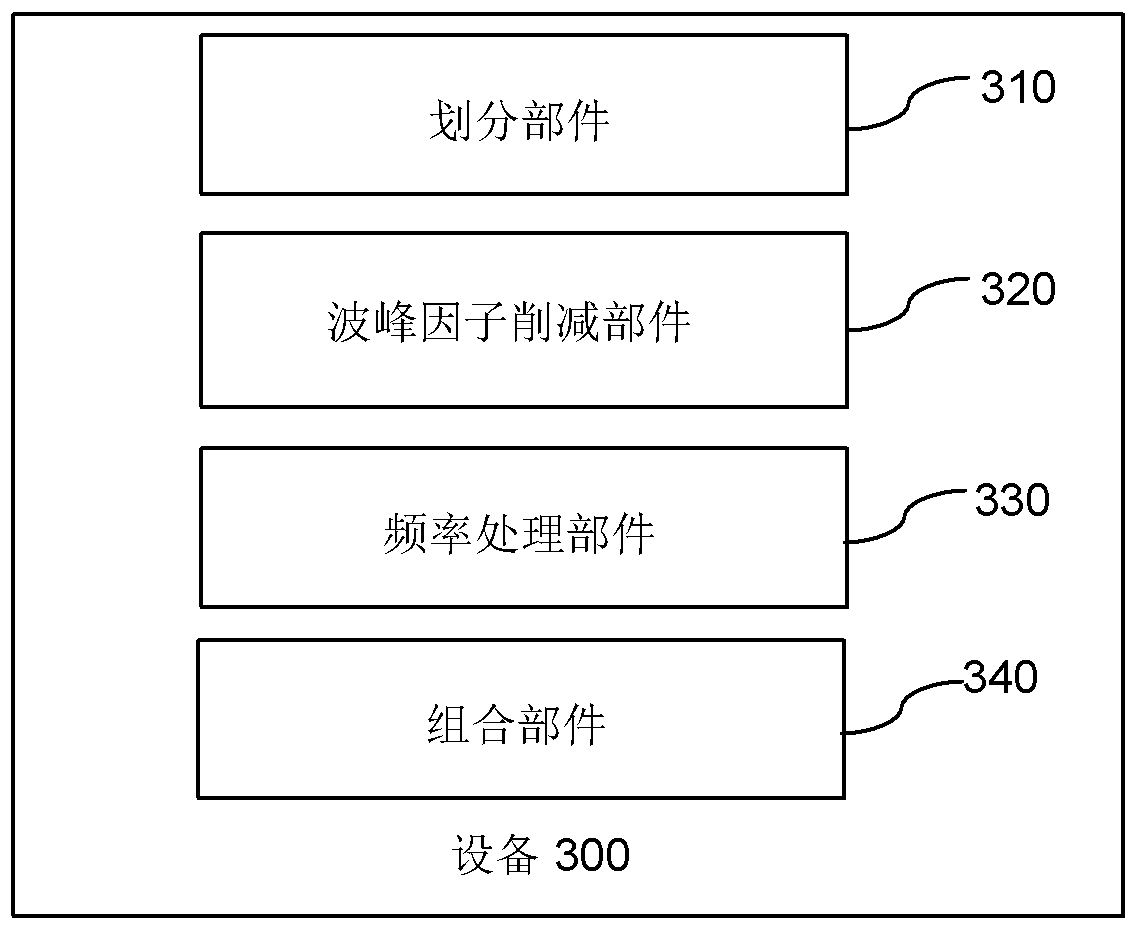
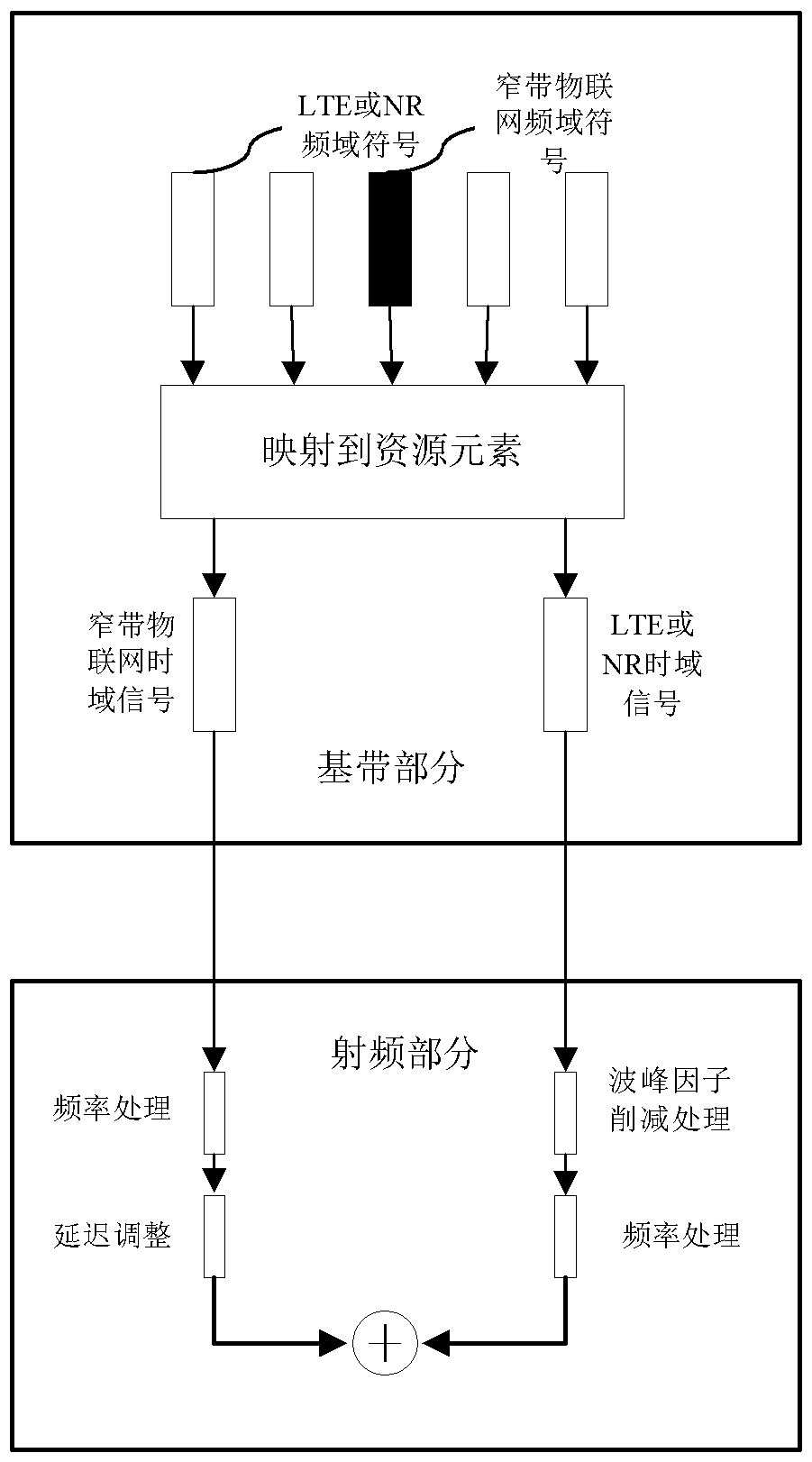
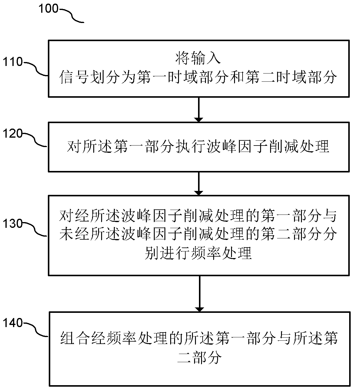
Image

Examples
Embodiment Construction
[0050] Hereinafter, the principle and spirit of the present disclosure will be described with reference to illustrative embodiments. It should be understood that all these embodiments are given only for the purpose of a person skilled in the art to better understand and further practice the present disclosure, and not for the purpose of limiting the scope of the present disclosure.
[0051] References to "one embodiment", "exemplary embodiment", etc. in the present disclosure indicate that the described embodiment may include specific features, structures, or characteristics, but it is not necessarily required that each embodiment includes the specific features , Structure, or characteristics. Furthermore, such phrases are not necessarily referring to the same embodiment.
[0052] It should be understood that although the terms "first" and "second" and so on may be used herein to describe various elements, these elements should not be limited by these terms. These terms are only ...
PUM
 Abstract
Description
Claims
Application Information
 - R&D
- Intellectual Property
- Life Sciences
- Materials
- Tech Scout
- Unparalleled Data Quality
- Higher Quality Content
- 60% Fewer Hallucinations
Browse by: Latest US Patents, China's latest patents, Technical Efficacy Thesaurus, Application Domain, Technology Topic, Popular Technical Reports.
© 2025 PatSnap. All rights reserved.Legal|Privacy policy|Modern Slavery Act Transparency Statement|Sitemap|About US| Contact US: help@patsnap.com