Semiconductor component test carrier, test apparatus thereof and equipment

A technology for component testing and conductor components, applied in the direction of single semiconductor device testing, measuring devices, measuring electricity, etc., can solve problems such as easy displacement or jumping out of the carrier plate 97, and achieve convenient feeding and discharging efficiency, fast feeding. The effect of feeding and discharging efficiency

Active Publication Date: 2019-07-16
KING YUAN ELECTRONICS
View PDF7 Cites 5 Cited by
  • Summary
  • Abstract
  • Description
  • Claims
  • Application Information

AI Technical Summary

Problems solved by technology

[0004] However, in this design, during the pressure test, the semiconductor element 96 is only placed on the carrier plate 97, without any measures to fix the semiconductor element 96, and the semiconductor element 96 is easily displaced during the rotation displacement process. Or jump out of the carrier plate 97, it is not very ideal, there is still room for improvement

Method used


Image

  • Semiconductor component test carrier, test apparatus thereof and equipment
  • Semiconductor component test carrier, test apparatus thereof and equipment
  • Semiconductor component test carrier, test apparatus thereof and equipment

Examples


Embodiment Construction

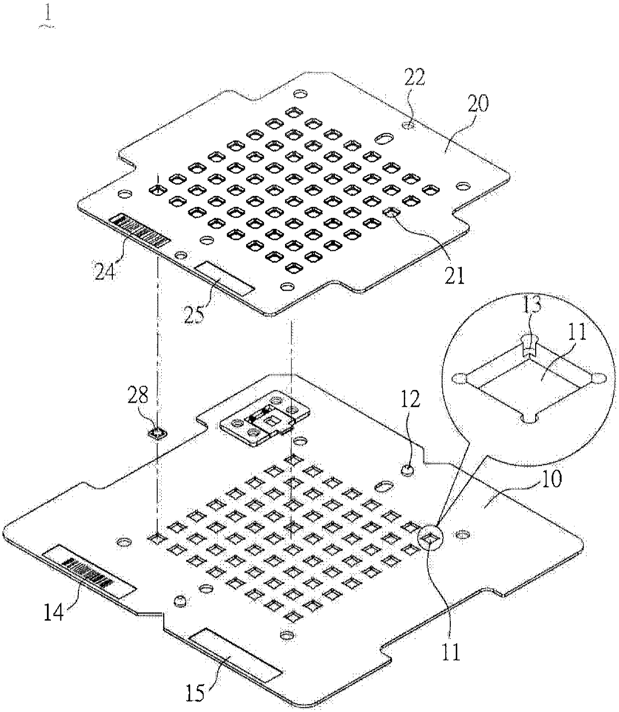
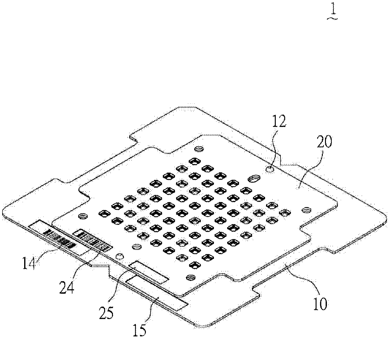
[0079] see figure 1 and figure 2 , which are respectively an exploded view and a perspective view of the semiconductor device test carrier according to the first preferred embodiment of the present invention. Shown in the figure is a semiconductor element test tray 1. The test tray 1 includes a bearing seat 10 and an upper cover 20. The bearing seat 10 has a plurality of through holes 11 and at least one positioning column 12. The upper surface of the bearing seat 10 is The surface has at least one groove 13 on the periphery of each through hole 11 for supporting a semiconductor element 28 . The upper cover 20 is covered on the bearing seat 10, and the upper cover 20 has a plurality of through holes 21 and at least one positioning hole 22, each through hole 21 corresponds to each through hole 11, and the at least one positioning hole 22 corresponds to the each through hole 11. At least one positioning column 12 is corresponding.

[0080] In this embodiment, the bearing ba...


PUM


Abstract

The invention relates to a semiconductor component test carrier, a test apparatus thereof and equipment. The semiconductor component test carrier comprises a carrying seat and an upper cover, whereinthe carrying seat is provided with a plurality of through holes and at least one positioning post; the upper surface of the carrying seat is provided with at least one groove at the periphery of eachthrough hole for carrying a semiconductor component; the upper cover covers the carrying seat; the upper cover is provided with a plurality of through holes and at least one positioning hole; each through hole in the upper cover corresponds to each through hole in the carrying seat; and the at least one positioning hole of the upper cover also corresponds to at least one positioning post of the carrying seat. Thus, during a sliding process of the test carrier, the semiconductor component does not shift or jump on the carrying seat.

Description

technical field [0001] The present invention relates to a semiconductor component test carrier and its testing device and equipment, especially to a semiconductor component suitable for testing, such as pressure sensor (Pressure Sensor), gas sensor (Gas Sensor), microphone (Microphone) and hygrometer (Humidity Sensor) and other sensing characteristics of the semiconductor element test carrier and its testing device and equipment. Background technique [0002] Existing technologies currently on the market, such as the semiconductor device testing device disclosed in US Patent Publication No. 2009 / 0015277 A1, please refer to Figure 13 A side view of an existing semiconductor device testing device. As shown in the figure, the test device described herein includes a first half cavity 91 and a second half cavity 92, wherein the first half cavity 91 is a fixed end, and the second half cavity 92 passes through a lifting device 90 moves vertically up and down to seal or separate t...

Claims


Application Information

Patent Timeline
Patent Type & Authority Applications(China)
IPC IPC(8): G01R31/26B07C5/34B07C5/36
CPCB07C5/34B07C5/362G01R31/2601
Inventor 丁伟修
Owner KING YUAN ELECTRONICS
Why Eureka
Try Eureka